Delay locked loop implementation in a synchronous dynamic random access memory
What is AI technical title?
AI technical title is built by Patsnap AI team. It summarizes the technical point description of the patent document.
a random access memory and lock loop technology, applied in the field of semiconductor memories, can solve the problems of limiting the limitation of the operating frequency of the part, and the pll solution also suffers from problems, so as to reduce the elapsed time, reduce the standby current and start-up time, and the effect of increasing the clock frequency
Inactive Publication Date: 2006-01-31
CONVERSANT INTPROP MANAGEMENT INC
View PDF61 Cites 111 Cited by
Summary
Abstract
Description
Claims
Application Information
AI Technical Summary
This helps you quickly interpret patents by identifying the three key elements:
Problems solved by technology
Method used
Benefits of technology
Benefits of technology
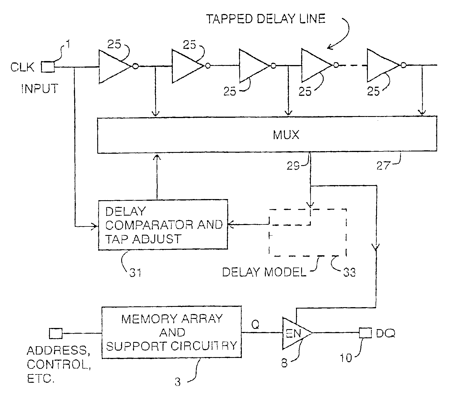
[0012]The present invention minimizes the elapsed time between a clock edge that is input to a synchronous memory such as an SDRAM and the time at which the same clock edge eventually triggers the output buffer of the SDRAM to drive valid data onto the outer terminals of the SDRAM. The present invention utilizes a delay locked loop (DLL) instead of the phase locked loop used in the second solution described above. The DLL allows higher clock frequency operation while requiring less standby current and start-up time than the system that uses the PLL. No oscillator is required as is required using the PLL, and the entire system can be fabricated using digital integrated circuit technology, rather than a mixture of analog and digital technology.
Problems solved by technology
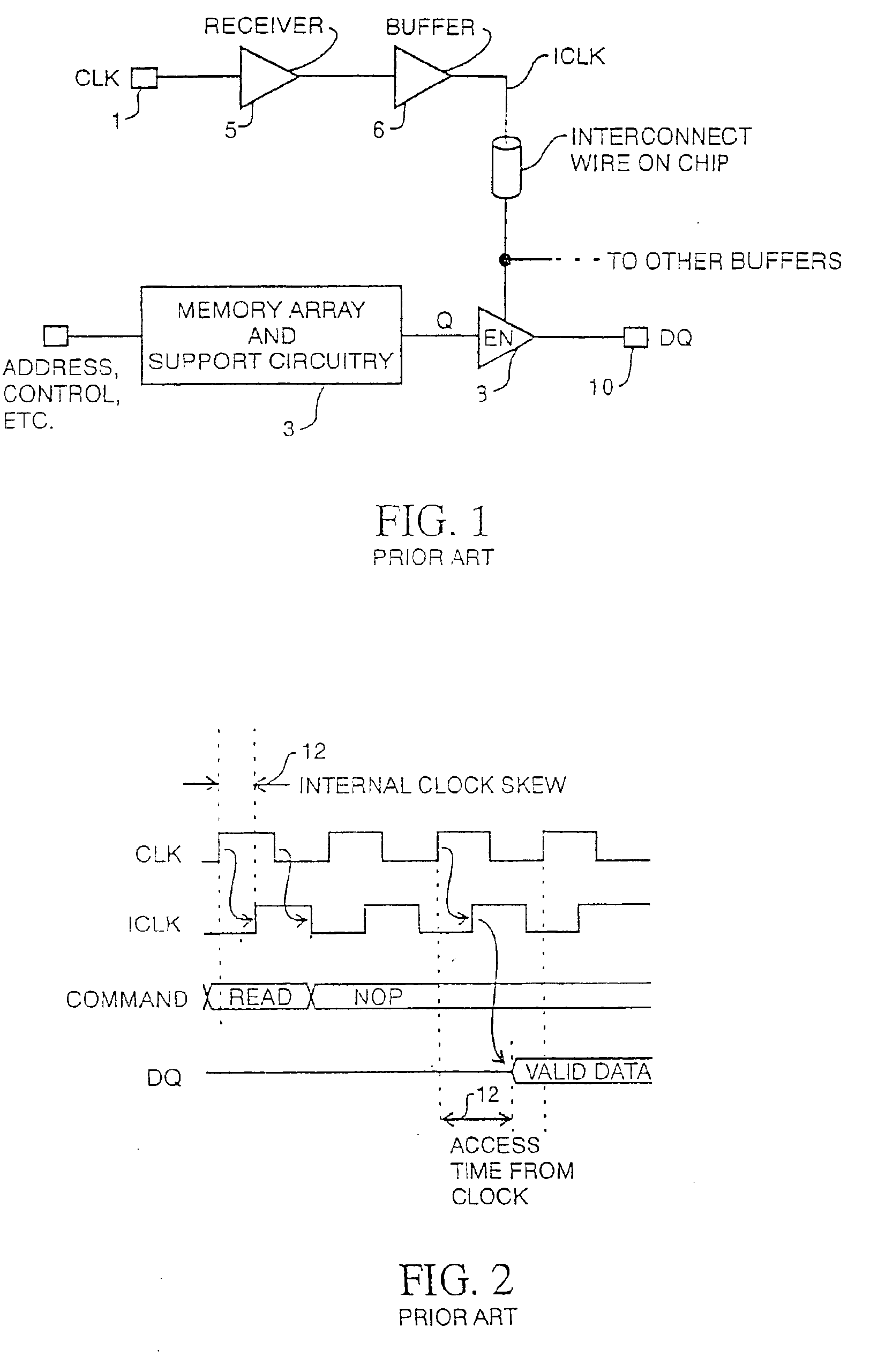
However, due to the delays caused by the internal buffering and the interconnect wire on the integrated circuit chip that distributes the clock signal, the clock signal arrives at the enable terminal of the buffers delayed from the clock input signal.
Implementing the first solution results in a limit to the operating frequency of the part.
There will always be a limit to the operating frequency of the part, because there will always be significant delay associated with the clock buffer and distribution circuitry and delay introduced by parasitic resistance and capacitance of the interconnection conductors used to distribute the buffered clock signal to the output buffers, which is evident from FIG.
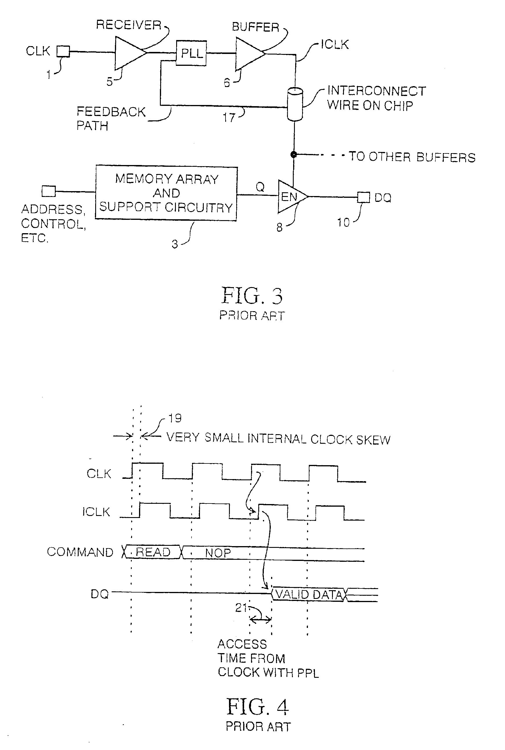
However it has been found that the PLL solution also suffers from problems.
It is complex, requiring an on-chip oscillator with feedback control of the frequency depending on the monitored status of the on-chip oscillator relative to the input clock.
It requires significant stand-by power due to its extra circuitry, and it requires considerable start-up time for the on-chip oscillator to synchronize and lock to the input clock frequency.
It also requires use of an analog oscillator in a digital circuit, which requires significantly different and complex fabrication techniques.
Method used
Image
Click on the blue label to locate the original text in one second.
Reading with bidirectional positioning of images and text.
Examples
Embodiment Construction
[0019]Turning to FIG. 5, an input clock signal is applied to a tapped delay line formed of a series of delay elements 25 such as inverters. The outputs of predetermined ones of the delay elements, which can be each one of the delay elements, are provided to the inputs of a selection apparatus such as a multiplexer 27. The output of the multiplexer 29 provides a signal, referred to herein as a driving clock signal, which in this embodiment is applied to the enable terminal of the output buffer in a manner as described above with respect to the prior art systems.
[0020]A delay comparator 31 has one input that receives the input clock signal, and another input that receives the driving clock signal. The comparator 31 outputs a control signal which has a value that depends on the differential between the input clock signal and the driving clock signal. That control signal is applied to the control inputs of multiplexer 27, and determines which of the inputs to it are passed through it to...
PUM
Abstract
A clock applying circuit for a synchronous memory is comprised of a clock input for receiving a clock input signal, apparatus connected to the synchronous memory for receiving a driving clock signal, and a tapped delay line for receiving the clock input signal and for delivering the clock driving signal to the synchronous memory in synchronism with but delayed from the clock input signal, the delay being a small fraction of the clock period of the clock input signal.
Description
RELATED APPLICATIONS[0001]This application is a Continuation of application Ser. No. 10 / 348,062, filed Jan. 17, 2003 now is Pat. No. 6,657,919, which is a Continuation of application Ser. No.10 / 279,217, filed Oct. 23, 2002 now U.S. Pat. No. 6,657,918, which is a Continuation of application Ser. No. 09 / 977,088, filed Oct. 12, 2001 now abandoned, which is a Continuation of application Ser. No. 09 / 761,274, filed Jan. 16, 2001, now U.S. Pat. No. 6,314,052, which is a Continuation of application Ser. No. 09 / 392,088, filed Sep. 8, 1999, now U.S. Pat. No. 6,205,083, which is a Continuation of application Ser. No. 08 / 996,095, filed Dec. 22, 1997, now U.S. Pat. No. 6,067,272, which is a Continuation of application Ser. No. 08 / 319,042, filed Oct. 6, 1994, now U.S. Pat. No. 5,796,673. The entire teachings of the above applications are incorporated herein by reference.FIELD OF THE INVENTION[0002]This invention relates to the field of semiconductor memories, and in particular to a circuit for ap...
Claims
Application Information
Patent Timeline
Application Date:The date an application was filed.
Publication Date:The date a patent or application was officially published.
First Publication Date:The earliest publication date of a patent with the same application number.
Issue Date:Publication date of the patent grant document.
PCT Entry Date:The Entry date of PCT National Phase.
Estimated Expiry Date:The statutory expiry date of a patent right according to the Patent Law, and it is the longest term of protection that the patent right can achieve without the termination of the patent right due to other reasons(Term extension factor has been taken into account ).
Invalid Date:Actual expiry date is based on effective date or publication date of legal transaction data of invalid patent.

