High speed circuitized substrate with reduced thru-hole stub, method for fabrication and information handling system utilizing same

a technology of circuitized substrates and throughholes, applied in the direction of high frequency circuit adaptations, line-transmission details, conductive pattern formation, etc., can solve the problems of low signal densities, low signal densities, and low performance of high-speed substrates such as those used for known chip carriers and multi-layered pcbs. to achieve the effect of eliminating signal loss, eliminating signal loss, and eliminating signal loss

Inactive Publication Date: 2006-02-07
TTM TECH NORTH AMERICA LLC +1
View PDF49 Cites 73 Cited by
  • Summary
  • Abstract
  • Description
  • Claims
  • Application Information

AI Technical Summary

Benefits of technology

[0024]It is, therefore, a primary object of the present invention to enhance the circuitized substrate art by providing such a substrate capable of high speed signal passage to interconnect electronic components mounted on the substrate.
[0026]According to one aspect of the invention, there is provided a high speed circuitized substrate comprising a plurality of electrically conductive layers, a plurality of dielectric layers alternately positioned between selected pairs of the electrically conductive layers and electrically insulating the conductive layers from each other, and a plurality of thru-holes spacedly positioned within the substrate and extending through selected ones of the dielectric layers and electrically conductive layers for electrically interconnecting selected ones of the electrically conductive layers to another of the electrically conductive layers to allow the passage of electrical signals between these interconnected electrically conductive layers. The electrical signals pass through the maximum length of the thru-holes so as to substantially eliminate signal loss due to thru-hole stub.
[0027]According to another aspect of the invention, there is provided a method of making a high speed circuitized substrate, the method comprising providing a plurality of electrically conductive layers, providing a plurality of dielectric layers and alternately positioning selected ones of these dielectric layers between selected pairs of the electrically conductive layers so as to electrically insulate the conductive layers from each other, forming a plurality of thru-holes within the substrate in a spaced orientation such that the plurality of thru-holes extend through selected ones of the dielectric and electrically conductive layers to electrically interconnect selected ones of the electrically conductive layers to another of the electrically conductive layers so as to allow the passage of electrical signals between these interconnected electrically conductive layers. The electrical signals pass through the maximum length of the thru-holes so as to substantially eliminate signal loss due to thru-hole stub.
[0028]According to yet another aspect of the invention, there is provided an electrical assembly comprising a high speed circuitized substrate including a plurality of electrically conductive layers, a plurality of dielectric layers alternately positioned between selected pairs of the electrically conductive layers and electrically insulating these conductive layers from each other, a plurality of thru-holes spacedly positioned within the substrate and extending through selected ones of the dielectric and electrically conductive layers for electrically interconnecting selected ones of the electrically conductive layers to another of the electrically conductive layers to allow the passage of electrical signals between these interconnected electrically conductive layers. The electrical signals pass through the maximum length of the thru-holes so as to substantially eliminate signal loss due to thru-hole stub. The assembly further includes at least one electrical component positioned on and electrically coupled to said circuitized substrate.
[0029]According to still another aspect of the invention, there is provided a high speed circuitized substrate assembly comprising a first high speed circuitized substrate including a first plurality of electrically conductive layers and a first plurality of dielectric layers alternately positioned between selected pairs of the first electrically conductive layers and electrically insulating the first electrically conductive layers from each other, a second high speed circuitized substrate including a second plurality of electrically conductive layers and a second plurality of dielectric layers alternately positioned between selected pairs of the second electrically conductive layers and electrically insulating the second electrically conductive layers from each other, the second circuitized substrate bonded to the first circuitized substrate to form a circuitized subassembly, and a plurality of thru-holes positioned with the high speed circuitized subassembly and electrically interconnecting selected ones of the first and second pluralities of electrically conductive layers to allow the passage of electrical signals between the interconnected electrically conductive layers. The electrical signals pass through the maximum length of the thru-holes so as to substantially eliminate signal loss due to thru-hole stub.
[0030]According to another aspect of the invention, there is provided an information handling system comprising a housing, a high speed circuitized substrate positioned within the housing and including a plurality of electrically conductive layers, a plurality of dielectric layers alternately positioned between selected pairs of the electrically conductive layers and electrically insulating these conductive layers from each other, a plurality of thru-holes spacedly positioned within the substrate and extending through selected ones of the dielectric and electrically conductive layers for electrically interconnecting selected ones of the electrically conductive layers to another of the electrically conductive layers to allow the passage of electrical signals between the interconnected electrically conductive layers, the electrical signals passing through the maximum length of the thru-holes so as to substantially eliminate signal loss due to thru-hole stub. This system further includes at least one electrical component positioned on and electrically coupled to the circuitized substrate.

Problems solved by technology

Such connections are subjected to the detrimental effects, e.g., signal deterioration, caused by the inherent characteristics of such known substrate wiring.
A typical high performance (high speed) substrate such as those used for known chip carriers and multilayered pcbs has not been able to provide wiring densities beyond a certain point due to limitations imposed by the direct current (dc) resistance maximum in connections between components (especially chips).
To produce a pcb with all wide lines would be impractical, primarily because of the resulting excessive thickness needed for the final board.
Such increased thicknesses are obviously unacceptable from a design standpoint.
As exemplified by the examples cited in the patents identified below, various alternative techniques have been used in an attempt to provide such high speed signal handling, but these also typically require unacceptable modifications to the substrate which are not conducive to mass production and / or a product of relatively simple construction.
As such, most of these also add to the final cost of the finished product.
From the above description, known substrates including such thru-holes typically suffer from the above mentioned via capacitance-signal degradation problem, which can be greatly amplified if the thru-holes used are of extended length and many signals pass there-over but only for a partial length thereof.
However, when signals do not pass along the entire length of the thru-hole, e.g., these pass to an internal conductive layer also coupled to the thru-hole but at only a partial depth thereof, there arises a signal“conflict” because part of the signal tends to traverse the remaining length (“stub”) of the thru-hole while another part will pass directly to the internal layer.
The result of this“conflict” is signal“noise” or loss, due to the “rebound” of the traversing part of the signal.
Consequently, re-reflections return from the junction to the branches, causing distortions in signals sensed at the devices.

Method used


Image

  • High speed circuitized substrate with reduced thru-hole stub, method for fabrication and information handling system utilizing same
  • High speed circuitized substrate with reduced thru-hole stub, method for fabrication and information handling system utilizing same
  • High speed circuitized substrate with reduced thru-hole stub, method for fabrication and information handling system utilizing same

Examples


Embodiment Construction

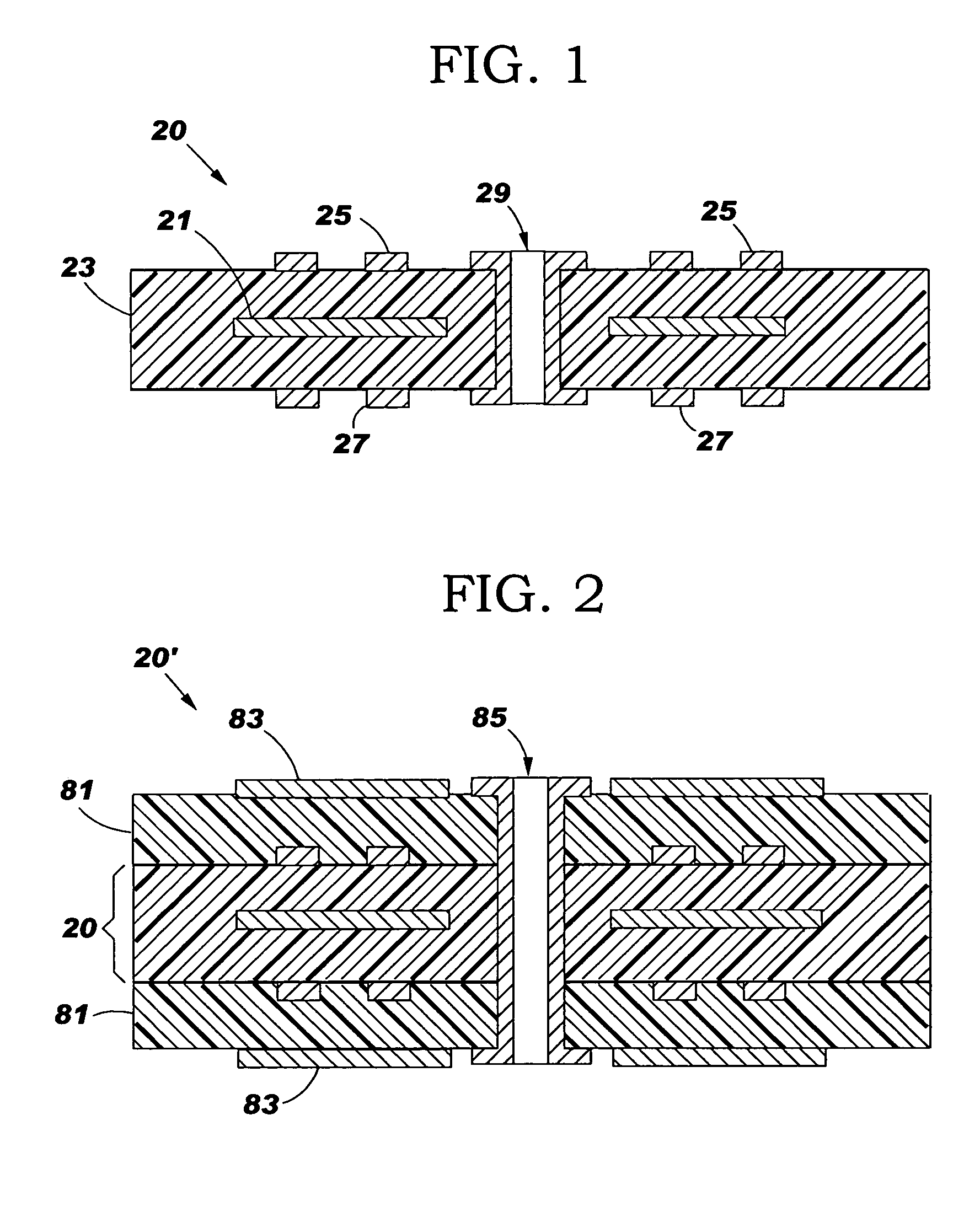
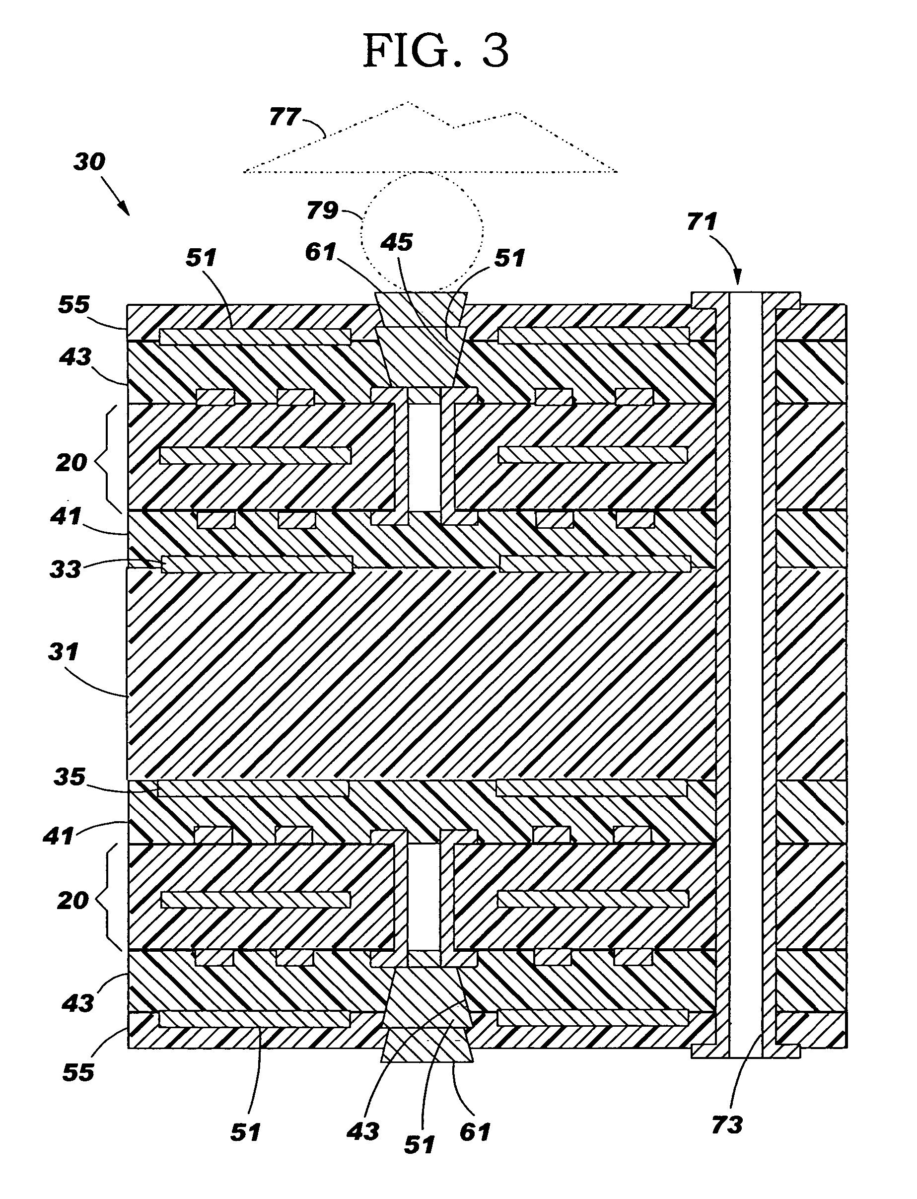
[0042]For a better understanding of the present invention, together with other and further objects, advantages and capabilities thereof, reference is made to the following disclosure and appended claims in connection with the above-described drawings. It is understood that like numerals will be used to indicate like elements from FIG. to FIG.

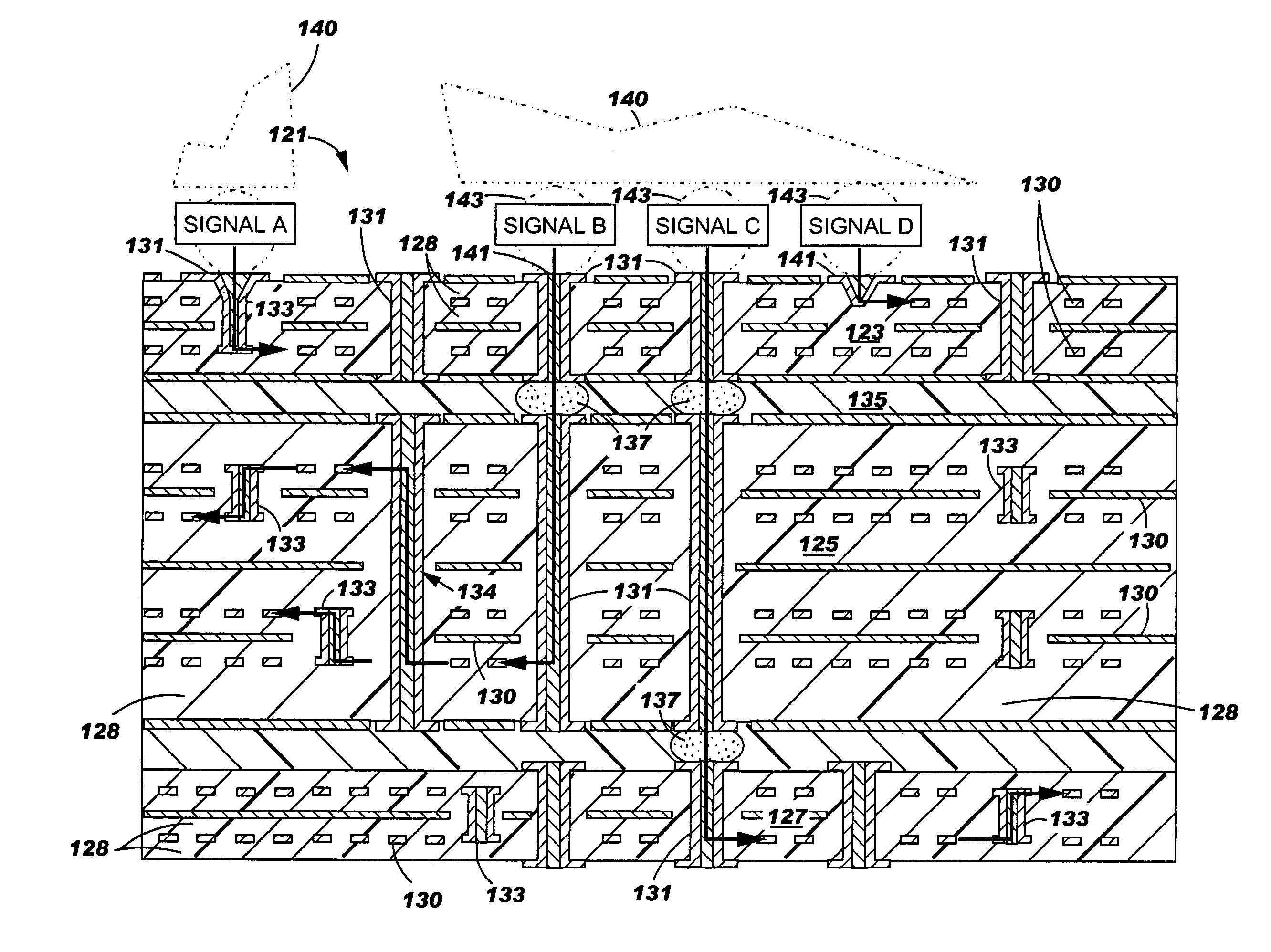
[0043]As stated above, the term“high speed” as used herein is meant signals of high frequency. Examples of such signal frequencies attainable for the circuitized substrates defined herein and as produced using the methods taught herein include those within the range of from about 3.0 to about 10.0 gigabits per second (Gb / s). These examples are not meant to limit this invention, however, because frequencies outside this range, including those higher, are attainable. As further understood from the following, the circuitized products produced herein may be formed of at least two separate layered portions which have themselves been formed prior to b...


PUM

PropertyMeasurementUnit
impedanceaaaaaaaaaa
thickaaaaaaaaaa
thickaaaaaaaaaa

Abstract

A circuitized substrate including a plurality of conductive and dielectric layers and also a plurality of conductive thru-holes therein for passing high speed signals, e.g., from one component to another mounted on the substrate. The substrate utilizes a signal routing pattern which uses the maximum length of each of the thru-holes wherever possible to thereby substantially eliminate signal loss (noise) due to thru-hole “stub” resonance. A multilayered circuitized substrate assembly using more than one circuitized substrate, an electrical assembly using a circuitized substrate and one or more electrical components, a method of making the circuitized substrate and an information handling system incorporating one or more circuitized substrate assemblies and attached components are also provided.

Description

CROSS REFERENCE TO CO-PENDING APPLICATION[0001]This is a continuation-in-part application of Ser. No. 10 / 354,000, filed Jan. 30, 2003 Now U.S. Pat. No. 6,828,514 and entitled “High Speed Circuit Board And Method For Fabrication” (inventors: B. Chan et al).TECHNICAL FIELD[0002]This invention relates to circuitized substrates, a prime example being multilayered printed circuit boards (pcbs), which include a plurality of thru-holes therein for providing interconnections between different conductive (e.g., signal) layers which form part of the substrate. The invention also relates to methods of making such substrates as well as various products (e.g., information handling systems) capable of utilizing such substrates as part thereof. Most particularly, the invention relates to such substrates, methods and products wherein the substrate is what is referred to as the high speed type.BACKGROUND OF THE INVENTION[0003]As operational requirements increase for electronic structures such as ele...

Claims


Application Information

Patent Timeline
Patent Type & Authority Patents(United States)
IPC IPC(8): H05K7/06H01L23/12H01L23/31H01L23/538H01L25/065H01L25/18H05K1/02H05K1/11H05K3/46
CPCH01L25/0652H01L25/0655H01L25/18H05K1/024H05K3/4623H05K3/4688H01L23/5383H01L23/3128Y10T29/49155H01L2224/16H01L2224/73253H01L2924/01046H01L2924/01057H01L2924/01078H01L2924/01079H01L2924/14H01L2924/1433H01L2924/15311H01L2924/16195H01L2924/3011H01L2924/3025H05K1/113H05K2201/09536H05K2201/096H05K2203/061H01L2924/01019H01L2924/01087H01L2224/16225H01L2224/32245Y10T29/49165
Inventor CHAN, BENSONLAUFFER, JOHN M.
Owner TTM TECH NORTH AMERICA LLC
Why Eureka
Try Eureka