Multibeam semiconductor laser, semiconductor light-emitting device and semiconductor device

a semiconductor laser and light-emitting device technology, applied in the direction of lasers, semiconductor laser arrangements, semiconductor lasers, etc., can solve the problems of difficult to employ the structure disclosed in this publication, and cannot be directly used as the light source of laser beam sprinters, so as to achieve the effect of easy examination

Inactive Publication Date: 2006-02-07
SONY CORP
View PDF18 Cites 136 Cited by
  • Summary
  • Abstract
  • Description
  • Claims
  • Application Information

AI Technical Summary

Benefits of technology

[0009]It is a more general object of the invention to provide a multi-beam semiconductor laser using nitride III–V compound semiconductors

Problems solved by technology

However, the two-beam semiconductor laser shown in FIG. 1 cannot drive individual laser structures independently, and it cannot be directly used as the light source of a laser beam sprinter.
However, it is difficult to employ the structure disclosed in this publication cannot d

Method used


Image

  • Multibeam semiconductor laser, semiconductor light-emitting device and semiconductor device
  • Multibeam semiconductor laser, semiconductor light-emitting device and semiconductor device
  • Multibeam semiconductor laser, semiconductor light-emitting device and semiconductor device

Examples


first embodiment

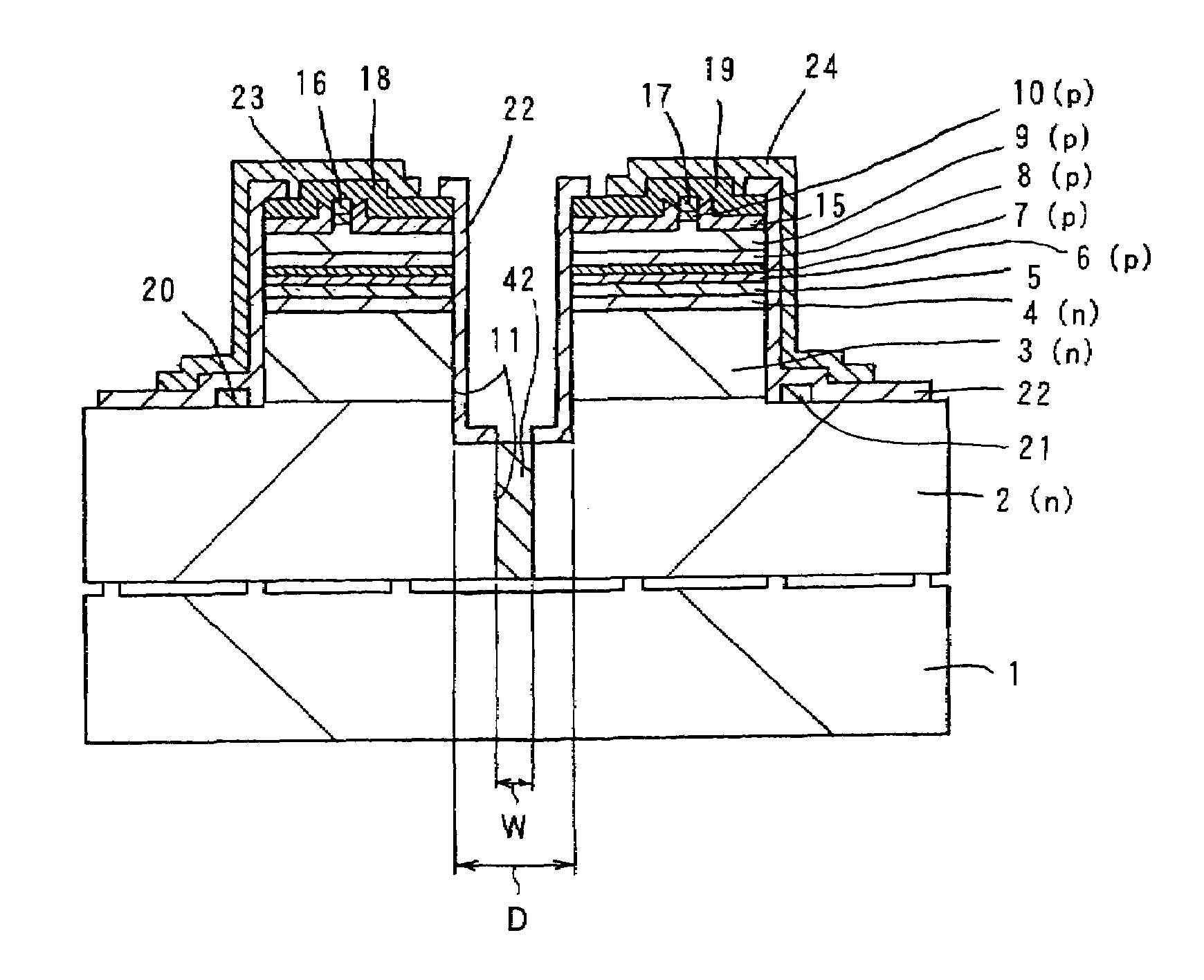
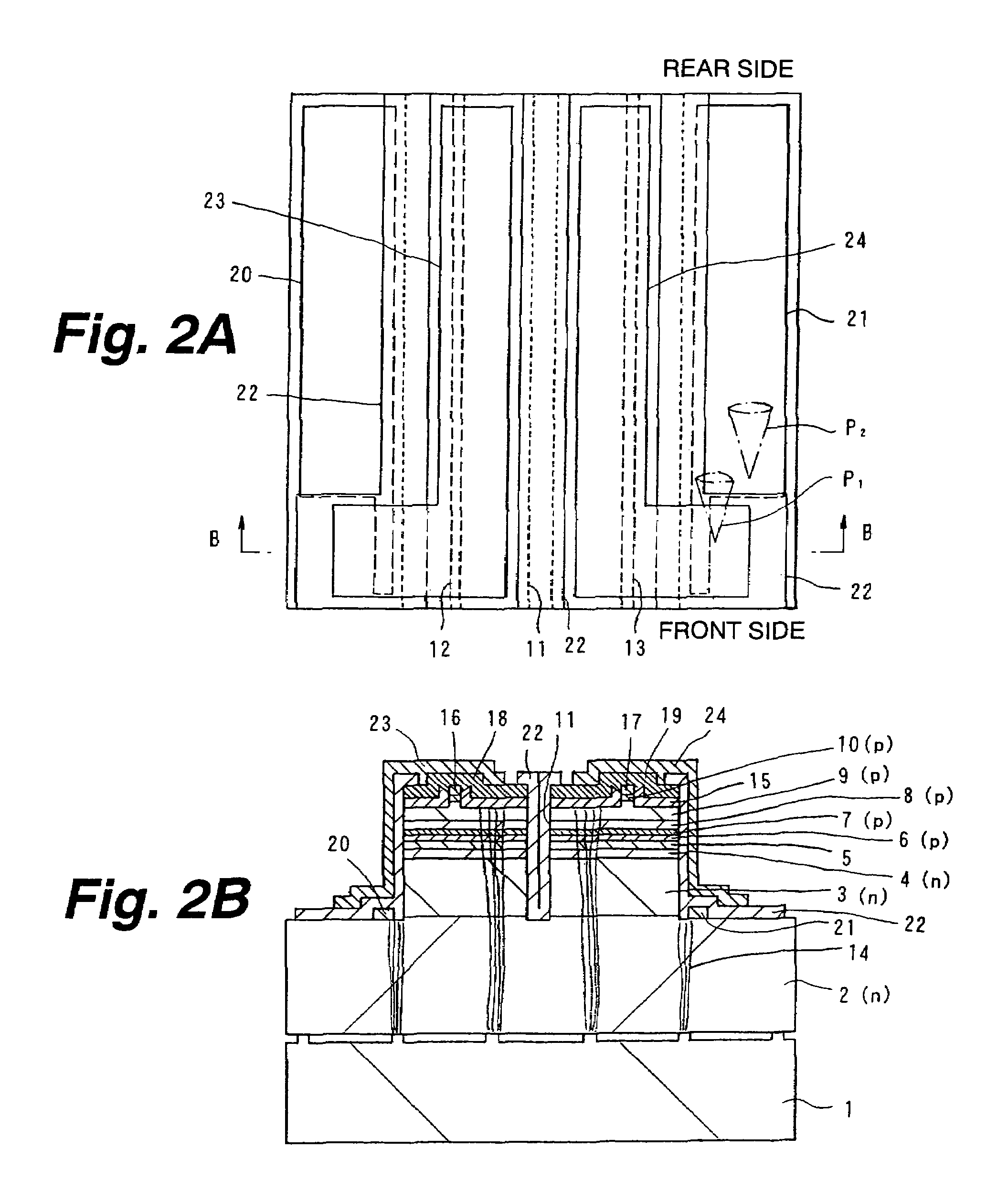
[0040]FIGS. 2A and 2B illustrate a two-beam GaN compound semiconductor laser (in form of a chip) according to the invention. FIG. 2A is a plan view, and FIG. 2B s a cross-sectional view taken along the B—B line of FIG. 1A. The two-beam GaN compound semiconductor laser is a real-indexed type semiconductor laser having a ridge structure and a SCH (Separate Confinement Heterostructure).

[0041]As shown in FIGS. 2A and 2B, the two-beam GaN compound semiconductor laser includes an n-type GaN layer 2 grown by a lateral crystal growth technique such as ELO (Epitaxial Lateral Overgrowth) on a c-plane sapphire substrate 1 via an undoped GaN buffer layer (not shown) formed by low-temperature growth. GaN compound semiconductor layers forming a laser structure are deposited on the n-type GaN layer 2. More specifically, there are sequentially deposited an n-type AlGaN clad layer 3, n-type GaN optical guide layer 4, active layer 5 having an undoped InxGa1−xN / INyGa1−yN multiquantum well structure, p...

second embodiment

[0068]Next explained is a two-beam GaN compound semiconductor laser according to the invention.

[0069]FIG. 3 is a cross-sectional view, similar to FIG. 2B, of the two-beam GaN compound semiconductor laser. The two-beam GaN compound semiconductor laser appears identically in its plan view.

[0070]As shown in FIG. 3, in the two-beam GaN compound semiconductor laser, the groove 11 for isolating two laser structures pass through the n-type GaN layer 2, and an insulating film 22 is formed to bury the groove.

[0071]The other features of this two-beam GaN compound semiconductor laser are identical to those of the first embodiment. So, their detailed explanation is omitted.

[0072]The second embodiment has the same advantages as those of the first embodiment, and additional advantages explained below. That is, since the groove 11 extends through the n-type GaN layer 2, there is no electrically conductive semiconductor layer connecting two laser structures exists. Therefore, two laser structures a...

third embodiment

[0074]Next explained is a four-beam GaN compound semiconductor laser according to the invention.

[0075]FIGS. 4A and 4B show the four-beam GaN compound semiconductor laser (still in form of a chip). FIG. 4A is a plan view, and FIG. 4B is a cross-sectional view taken along the B—B line of FIG. 4A.

[0076]As shown in FIGS. 4A and 4B, the four-beam GaN compound semiconductor laser includes four isolated laser structures in correspondence to four beams. In the following explanation, these four laser structures are numbered first to fourth in order from the left end one in FIGS. 4A and 4B. Reference numerals 25 through 28 denote ridges of these four laser structures. Distance between every adjacent two of the ridges 25 through 28 is 16 μm for example.

[0077]In the first laser structure, a p-side electrode 29 comprising a Pd film and a Pt film, for example, stacked sequentially is formed in contact with the p-type GaN contact layer 10 of the ridge 25. Further formed thereon is a p-side electro...


PUM


Abstract

In a multi-beam semiconductor laser including nitride III–V compound semiconductor layers stacked on one surface of a substrate of sapphire or other material to form laser structures, and including a plurality of anode electrodes and a plurality of cathode electrodes formed on the nitride III–V compound semiconductor layers, one of the anode electrodes is formed to bridge over one of the cathode electrodes via an insulating film, and another anode electrode is formed to bridge over another of the cathode electrodes via an insulating film.

Description

[0001]This application claims priority to Japanese Patent Application Number JP2002-168945, filed Jun. 10, 2002 which is incorporated herein by reference.Technical Field[0002]This invention relates to a multi-beam semiconductor laser, semiconductor light-emitting device and semiconductor device, suitable for application to a multi-beam semiconductor laser using nitride III–V compound semiconductors for example.BACKGROUND ART[0003]As semiconductor lasers using nitride III–V compound semiconductors such as AlGaInN, single beam type lasers have been developed and has entered a phase of practical applications as light sources of high-density optical discs, and the like.[0004]On the other hand, for application of a semiconductor laser using nitride III–V compound semiconductors to a light source of a laser beam printer, it is necessary to realize a multi-beam semiconductor laser in which two beams or four beams can be driven independently.[0005]The Applicant proposed a two-beam semicondu...

Claims


Application Information

Patent Timeline
IPC IPC(8): H01L33/00H01S5/042H01S5/22H01S5/323H01S5/343H01S5/40
CPCB82Y20/00H01S5/4031H01S5/042H01S5/0421H01S5/02276H01S5/34333H01S5/0425H01L2224/18H01L2224/73267H01L2224/24137H01S5/04257H01S5/04256H01S5/02345H01S5/22
Inventor TOJO, TSUYOSHIYABUKI, YOSHIFUMIANSAI, SHINICHIHINO, TOMONORIGOTO, OSAMUFUJIMOTO, TSUYOSHIMATSUMOTO, OSAMUTAKEYA, MOTONOBUOOFUJI, YOSHIO
Owner SONY CORP
Why Eureka
Try Eureka