CMP apparatus polishing head with concentric pressure zones

Inactive Publication Date: 2006-02-14
TAIWAN SEMICON MFG CO LTD
View PDF9 Cites 9 Cited by
  • Summary
  • Abstract
  • Description
  • Claims
  • Application Information

AI Technical Summary

Benefits of technology

[0018]In accordance with these and other objects and advantages, the present invention is directed to a CMP polishing head having multiple concentric pressure zones for selectively increasing polishing pressure against selected regions of a semiconductor wafer in order to compensate for variations in polishing rates on the wafer surface otherwise caused by ridges or other non-uniformities in the wafer surface. The polishing head of the present invention comprises multiple, concentric, inflatable pressure rings each of which may be selectively inflated to increase the polishing pressure against a concentric ridge or material elevation on the corresponding concentric region of the wafer surface and increase the polishing rate of the concentric ridge or elevation between the rotating polishing head and a stationary polishing pad. A channel selector is typically included in the polishing head for selectively aligning an air / pressure vacuum source with a selected one of multiple pressure tubes that connect to the respective pressure rings.

Problems solved by technology

The amount of the dielectric material removed is normally between about 5000 A and about 10,000 A. The uniformity requirement for ILD or IMD polishing is very stringent since non-uniform dielectric films lead to poor lithography and resulting window-etching or plug-formation difficulties.
A thickness variation across the wafer is therefore produced as a major cause for wafer non-uniformity.
In the improved CMP head design, even though a pneumatic system for forcing the wafer surface onto a polishing pad is used, the system cannot selectively apply different pressures at different locations on the surface of the wafer.
Accordingly, while the CMP process provides a number of advantages over the traditional mechanical abrasion type polishing process, a serious drawback for the CMP process is the difficulty in controlling polishing rates at different locations on a wafer surface.

Method used


Image

  • CMP apparatus polishing head with concentric pressure zones
  • CMP apparatus polishing head with concentric pressure zones
  • CMP apparatus polishing head with concentric pressure zones

Examples


Embodiment Construction

[0030]The present invention has particularly beneficial utility in the uniform polishing of semiconductor wafers having a non-uniform surface in the semiconductor fabrication industry. However, the invention is not so limited in application, and while references may be made to such semiconductor wafers, the present invention is more generally applicable to polishing substrates in a variety of mechanical and industrial applications.

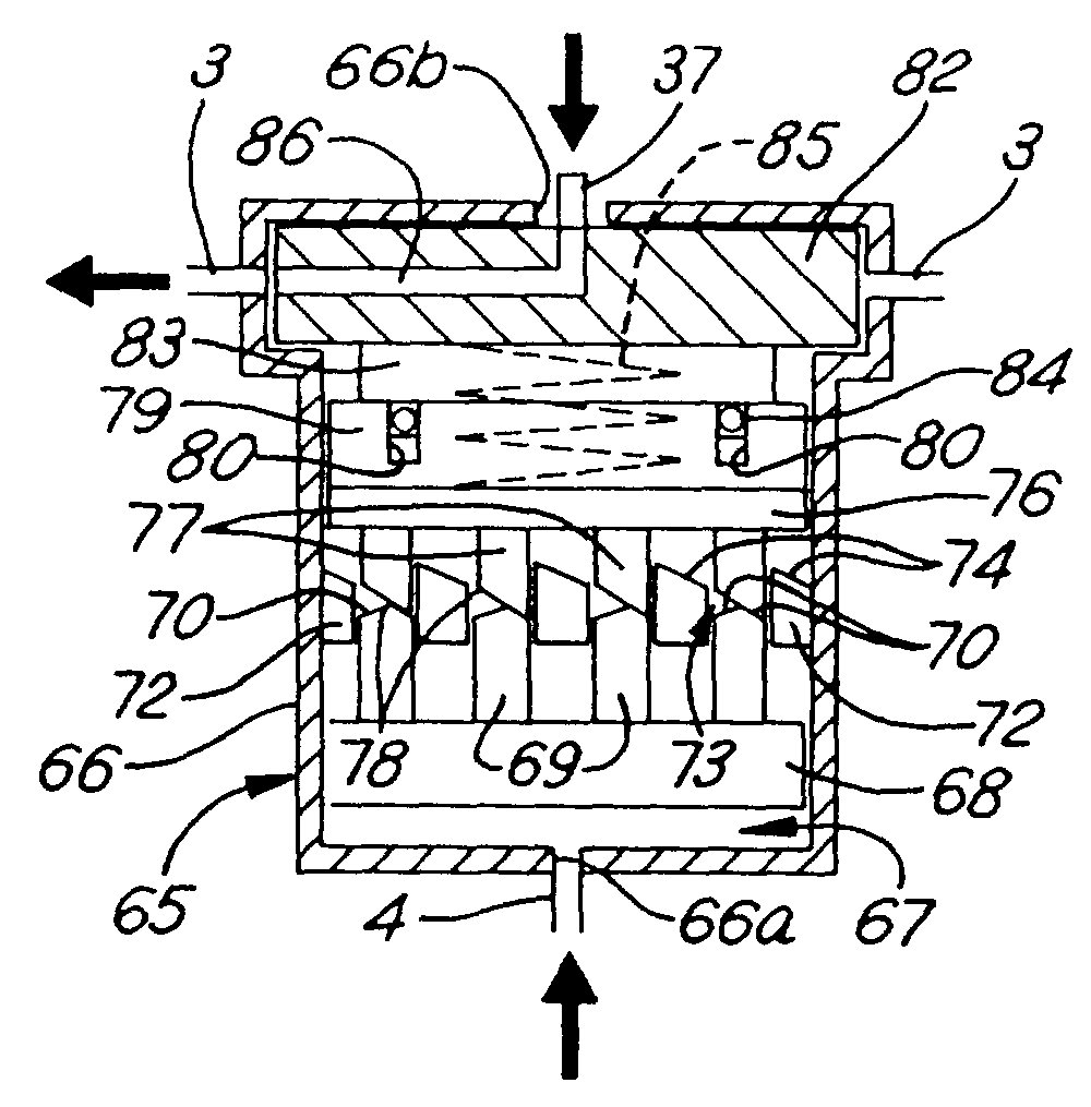
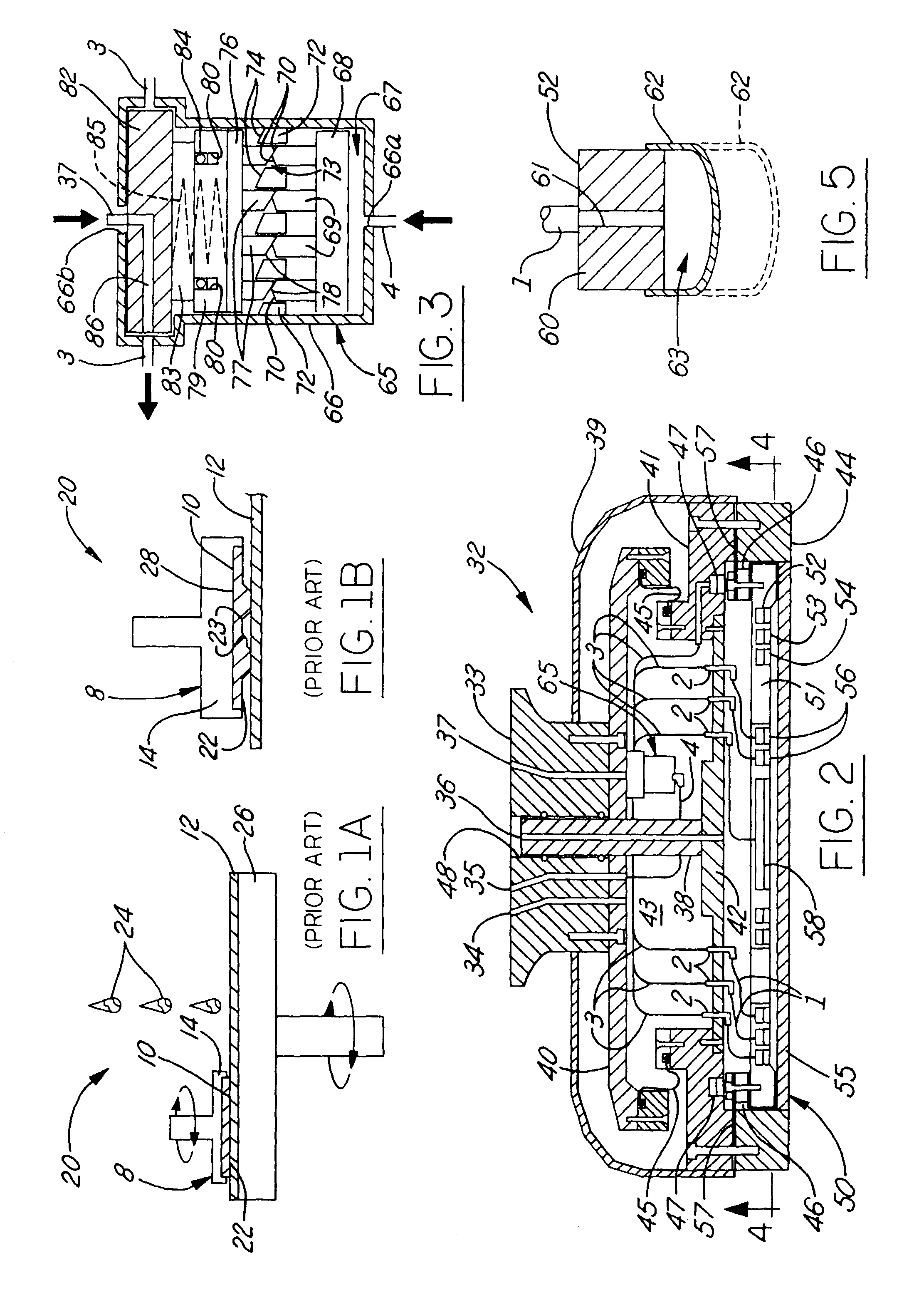
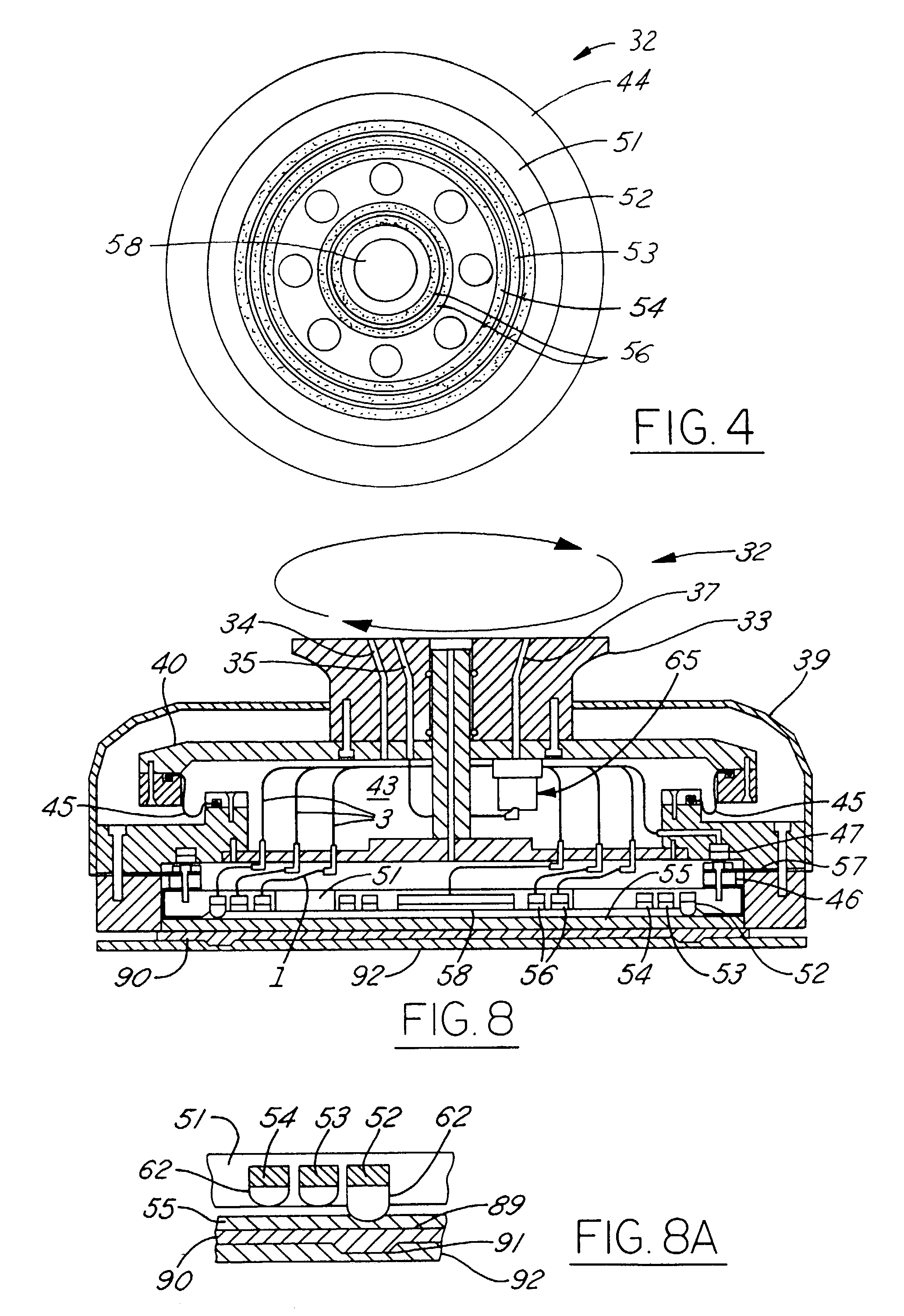
[0031]Referring initially to FIG. 2, a polishing head 32 of the present invention includes a housing 39 which is connected to a hub 33 supported on a drive shaft (not shown) to rotate therewith during polishing about an axis of rotation which is substantially perpendicular to the surface of a polishing pad (not shown) during polishing, as hereinafter described. The housing 39 may be circular in shape to correspond to the circular configuration of the substrate to be polished. A cylindrical bushing 48 may fit into a vertical bore extending through the hub 3...


PUM

PropertyMeasurementUnit
Pressureaaaaaaaaaa
Flexibilityaaaaaaaaaa

Abstract

A CMP polishing head having multiple concentric pressure zones for selectively increasing polishing pressure against selected regions of a semiconductor wafer in order to compensate for variations in polishing rates on the wafer surface otherwise caused by ridges or other non-uniformities in the wafer surface. The polishing head of the present invention comprises multiple, concentric, inflatable pressure rings each of which may be selectively inflated to increase the polishing pressure against a concentric ridge or material elevation on the corresponding concentric region of the wafer surface and increase the polishing rate of the concentric ridge or elevation between the rotating polishing head and a stationary polishing pad. A channel selector may be included in the polishing head for selectively aligning an air / pressure vacuum source with a selected one of multiple pressure tubes that connect to the respective pressure rings.

Description

FIELD OF THE INVENTION[0001]The present invention relates to chemical mechanical polishing apparatus used in the polishing of semiconductor wafers. More particularly, the present invention relates to a CMP apparatus polishing head which includes multiple concentric pressure zones for applying variable polishing pressure against various regions on a semiconductor wafer.BACKGROUND OF THE INVENTION[0002]In the fabrication of semiconductor devices from a silicon wafer, a variety of semiconductor processing equipment and tools are utilized. One of these processing tools is used for polishing thin, flat semiconductor wafers to obtain a planarized surface. A planarized surface is highly desirable on a shadow trench isolation (STI) layer, inter-layer dielectric (ILD) or on an inter-metal dielectric (IMD) layer, which are frequently used in memory devices. The planarization process is important since it enables the subsequent use of a high-resolution lithographic process to fabricate the nex...

Claims


Application Information

Patent Timeline
IPC IPC(8): B24B49/00B24B37/30B24B49/16
CPCB24B49/16B24B37/30
Inventor JAN, CHIN-TSANWU, JIANN-LIH
Owner TAIWAN SEMICON MFG CO LTD
Why Eureka
Try Eureka