

Polishing pad, process for preparing the same, and process for preparing a semiconductor device using the same
- Summary
- Abstract
- Description
- Claims
- Application Information
AI Technical Summary
Benefits of technology
Problems solved by technology
Method used
Image

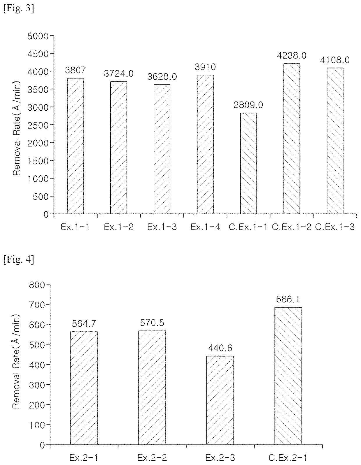
Examples
example 1-1
[0179](1) Preparation of a Urethane-Based Prepolymer
[0180]A four-necked flask was charged with a diisocyanate compound, polytetramethylene glycol (PTMG) as a polymer-type polyol and diethylene glycol (DEG) as a single-molecule-type polyol, which mixture was reacted at 80° C. for 2 hours to prepare a urethane-based prepolymer. The contents of the diisocyanate compound and the polyols are shown in Table 1-1.
[0181](2) Preparation of a Polishing Pad
[0182]A casting machine equipped with tanks and feeding lines for the raw materials such as a urethane-based prepolymer, a curing agent, and a foaming agent was provided. The urethane-based prepolymer prepared above, 4,4′-methylenebis(2-chloroaniline) (MOCA, Ishihara) as a curing agent, and a solid phase foaming agent (Akzonobel) were charged to each tank. The raw materials were stirred while they were fed to the mixing head at constant rates through the respective feeding lines. In such event, the prepolymer and the curing agent were fed at ...
examples 1-2 to 1-4
[0185]The same procedures as in Example 1-1 were carried out to obtain a polishing pad except that the contents of the respective components were changed as shown in Table 1-1 below.
example 2-1
[0186](1) Preparation of a Urethane-Based Prepolymer
[0187]A four-necked flask was charged with toluene 2,4-diisocyanate (2,4-TDI) as an aromatic diisocyanate compound, 4,4′-dicyclohexylmethane diisocyanate (H12MDI) as an alicyclic diisocyanate compound, and diethylene glycol (DEG) as a polyol, which mixture was reacted at 80° C. for 2 hours to prepare a urethane-based prepolymer. The contents of the aromatic diisocyanate compound, the alicyclic diisocyanate compound, and the polyol are shown in Table 2-1.
[0188](2) Preparation of a Polishing Pad
[0189]A casting machine equipped with tanks and feeding lines for the raw materials such as a urethane-based prepolymer, a curing agent, and a foaming agent was provided. The urethane-based prepolymer prepared above, 4,4′-methylenebis(2-chloroaniline) (MOCA, Ishihara) as a curing agent, and a solid phase foaming agent (Akzonobel) were charged to each tank. The raw materials were stirred while they were fed to the mixing head at constant rates ...
PUM
| Property | Measurement | Unit |
|---|---|---|
| Fraction | aaaaa | aaaaa |
| Percent by mass | aaaaa | aaaaa |
| Percent by mass | aaaaa | aaaaa |
Abstract
Description
Claims
Application Information