Semiconductor device

Inactive Publication Date: 2008-06-19
NEC ELECTRONICS CORP
View PDF15 Cites 1 Cited by
  • Summary
  • Abstract
  • Description
  • Claims
  • Application Information

AI Technical Summary

Benefits of technology

[0011]With the semiconductor device, the flange is warped arcuately against the substrate, as seen in the side view. Accordingly, it follows that there exist parts narrower in a spacing between the flange, and the wiring substrate as well as parts wider in a spacing therebetween. Therefore, providing the latter with through-holes, respectively, and providing the former with a binder can reduce a thickness of the binder while sufficiently securing respective sizes of the through-holes. Thereby, adhesion strength of the bonded parts between the lid and the wiring substrate is enhanced.
[0012]With the invention, it is possible to implement a semiconductor device excellent in reliability.

Problems solved by technology

Now, if space exists on the inner side of the lid 101, as shown in FIG. 7, there is the risk that moisture making the ingress into the space undergoes vaporization due to heating upon the mounting to thereby cause a sharp rise in internal pressure, resulting in rupture of the lid 101.
However, if the binder is increased in thickness, there occur cases where the binder itself is broken down under a load lower than a load causing exfoliation at bonded areas when an external force is applied.
As a result, there occurs deterioration in adhesion strength of the bonded parts between the lid and the substrate, which will lead to deterioration in reliability of the semiconductor device.

Method used


Image

  • Semiconductor device
  • Semiconductor device
  • Semiconductor device

Examples


first embodiment

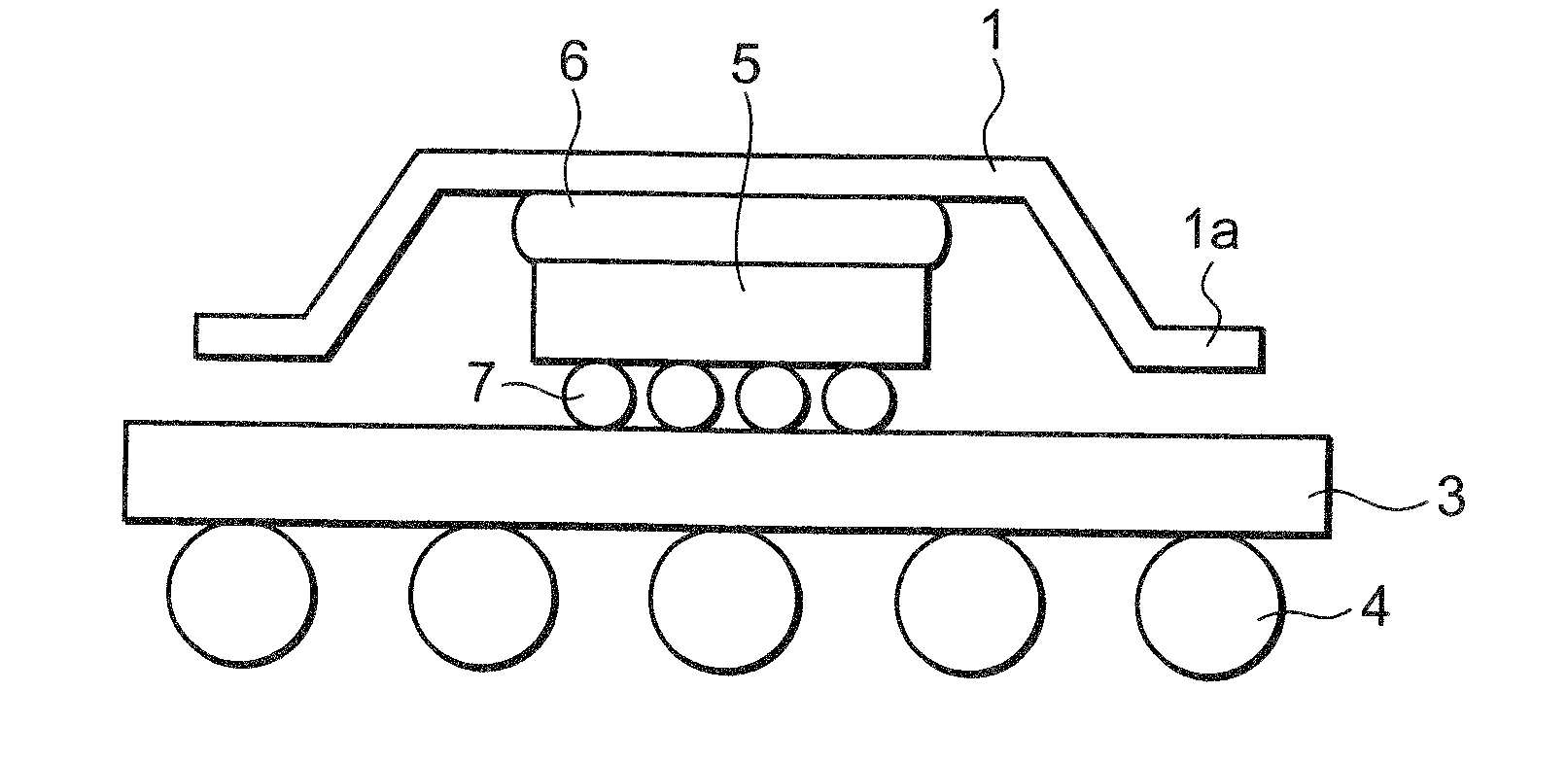
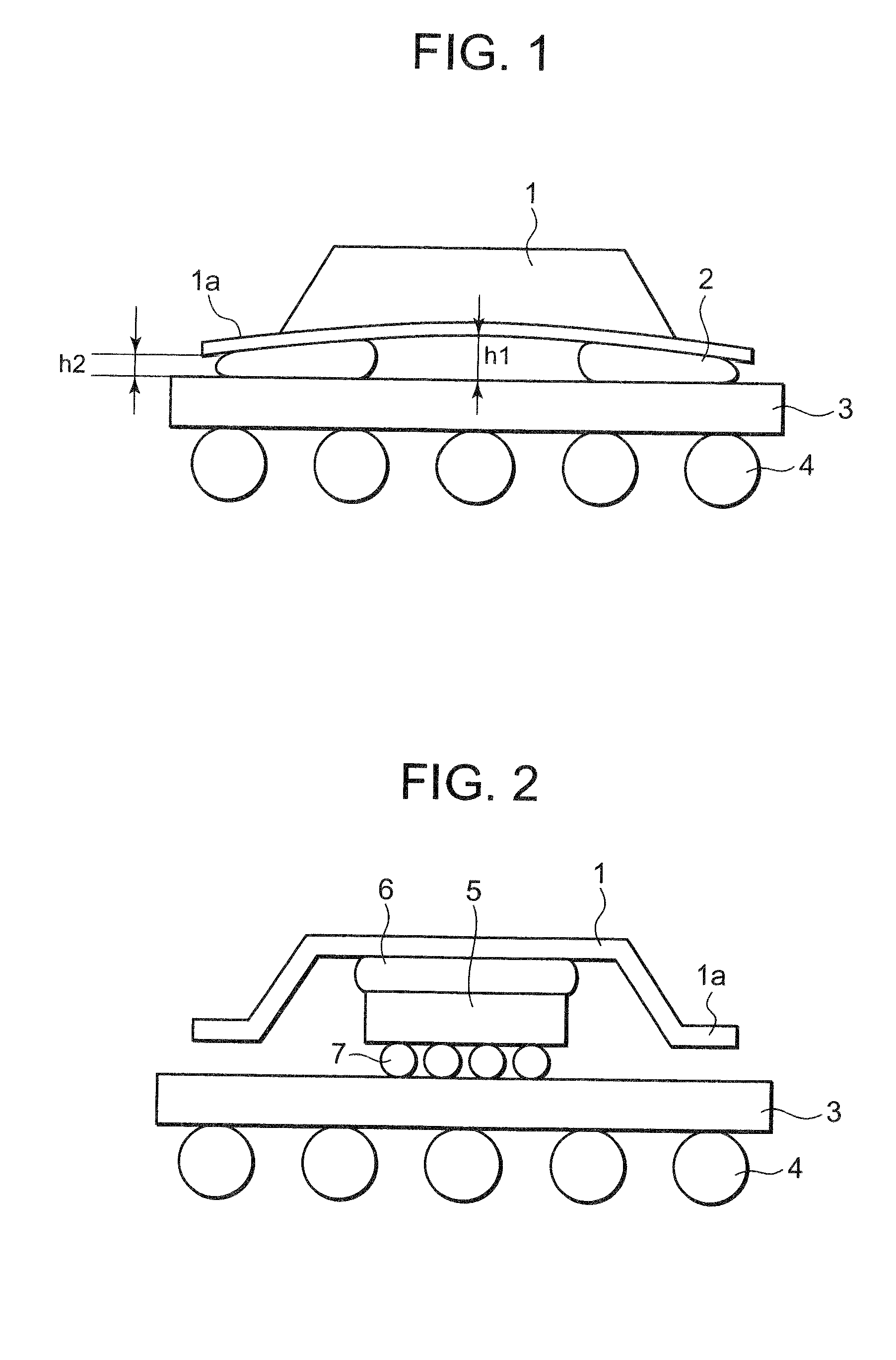
[0022]FIGS. 1 and 2 are a side view, and a sectional view, respectively, broadly showing a first embodiment of a semiconductor device according to the invention. The semiconductor device is provided with a substrate, for example, a wiring substrate 3, a semiconductor chip 5 mounted face down on the top of the wiring substrate 3, and a lid 1 having a depressed part for accommodating the semiconductor chip 5, and a flange 1a linked with the depressed part. Parts of the flange 1a (an edge thereof in the case of the present embodiment) of the lid 1 are bonded to the wiring substrate 3 by means of a binder 2. External terminals 4 are connected to the underside surface of the substrate 3.

[0023]As shown in FIG. 1, the flange 1a is warped arcuately against the substrate 3, as seen in the side view. In the present embodiment, in particular, the flange 1a is warped in such a fashion as to protrude against the substrate 3, as seen in the side view. As a result, in the side view, a spacing h1 b...

second embodiment

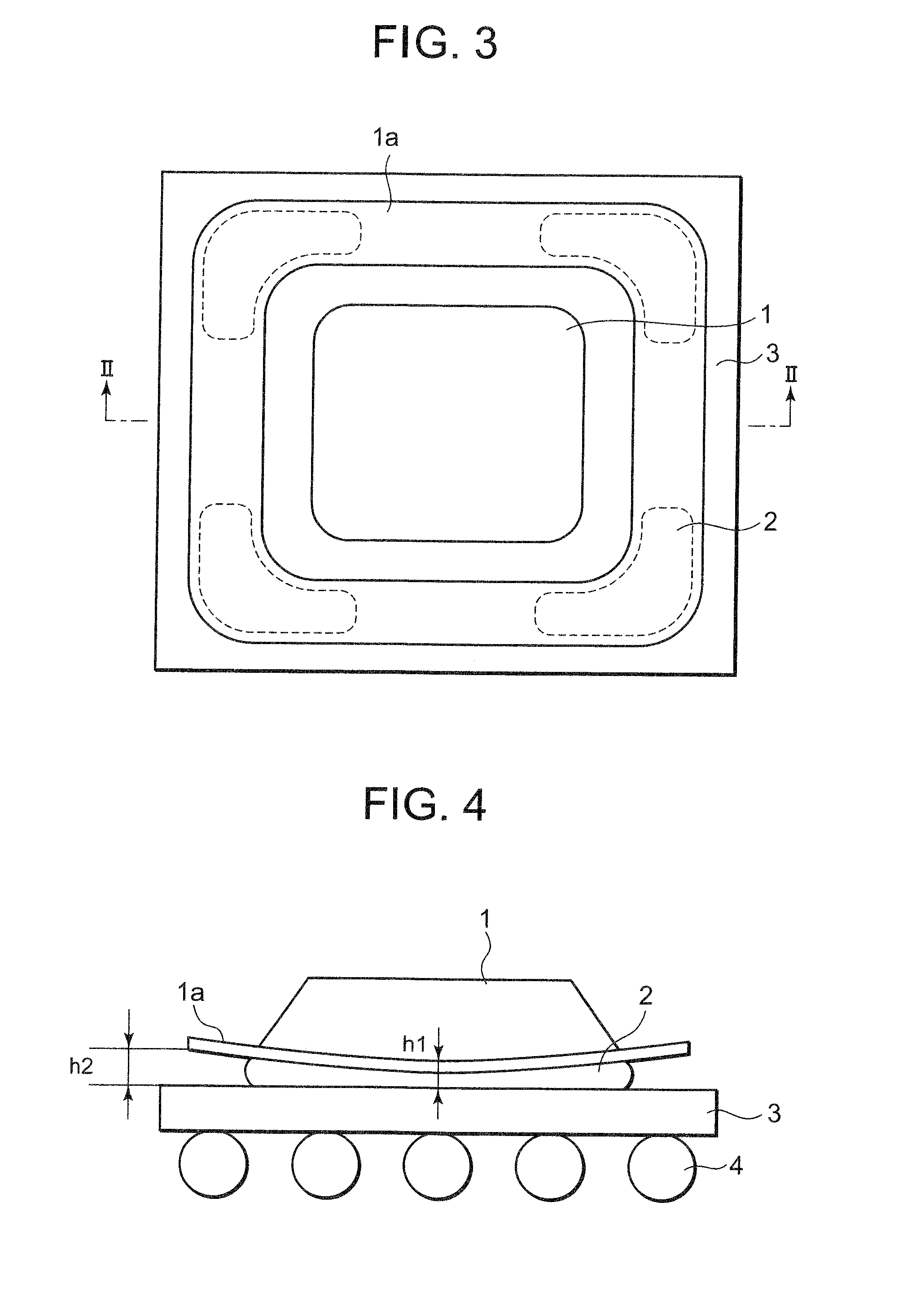
[0031]FIGS. 4 and 5 are a side view, and a sectional view, respectively, broadly showing a second embodiment of a semiconductor device according to the invention. The semiconductor device is provided with a wiring substrate 3, a semiconductor chip 5 mounted face down on the wiring substrate 3, and a lid 1 having a depressed part for accommodating the semiconductor chip 5, and a flange 1a linked with the depressed part. A part (a central part in the case of the present embodiment) of the flange 1a of the lid 1 is bonded to the wiring substrate 3 by means of the binder 2.

[0032]As shown in FIG. 4, the flange 1a is warped arcuately against the substrate 3, as seen in the side view. In the present embodiment, in particular, the flange 1a is warped in such a fashion as to be concaved against the substrate 3, as seen in the side view. As a result, in the side view, a spacing h1 between the center of the flange 1a, and the wiring substrate 3 is narrower than a spacing h2 between the edge of...


PUM


Abstract

With a conventional semiconductor device, there occurs deterioration in adhesion strength of bonded parts between a lid and a substrate. A semiconductor device according to an embodiment of the invention includes a substrate, a semiconductor chip with one of surfaces thereof, facing downward, mounted on the substrate, and a lid having a depressed part for accommodating the semiconductor chip, and a flange linked with the depressed part. Parts of the flange of the lid are bonded to the substrate by means of a binder. The flange is warped arcuately against the substrate, as seen in a side view. The bottom surface of the depressed part of the lid is bonded to the other surface of the semiconductor chip by means of a binder.

Description

FIELD OF THE INVENTION[0001]The present invention relates to a semiconductor device.BACKGROUND OF THE INVENTION[0002]Enhancement in working speed of a high-performance semiconductor device available lately has been accompanied by an increase in heating value thereof. In order to cope with such a trend, a technology called flip chip mounting has been put to use in a semiconductor package (hereinafter referred to as a package) with increasing frequency.[0003]FIG. 7 is a sectional view showing a conventional semiconductor device using the flip chip mounting. With this semiconductor device, use is made of a method whereby electrode terminals of a semiconductor chip 105 are positioned opposite to electrode terminals of a substrate 103, respectively, so as to be bonded with each other through the intermediary of bumps 107 formed on the tops of the respective electrode terminals of the semiconductor chip 105. External terminals 104 are connected to the underside surface of the substrate 10...

Claims


Application Information

Patent Timeline
IPC IPC(8): H01L23/02
CPCH01L23/04H01L23/10H01L23/42H01L2224/16H01L2224/73253H01L2924/01078H01L2924/3511H01L2924/01079H01L2924/15311H01L2924/16152H01L2924/00011H01L2924/00014H01L2224/0401
Inventor MIZUNASHI, HARUMI
Owner NEC ELECTRONICS CORP
Why Eureka
Try Eureka