Organic electroluminescent device and fabricating method thereof

an electroluminescent device and organic technology, applied in the field of semiconductor devices, can solve the problems of shortening the expected life span of organic elds, affecting the appearance of organic elds, and requiring a relatively high amount of power to operate, so as to reduce the probability of line defects, improve the aperture ratio, and increase the expected life of devices

Inactive Publication Date: 2006-02-14
LG DISPLAY CO LTD
View PDF9 Cites 18 Cited by
  • Summary
  • Abstract
  • Description
  • Claims
  • Application Information

AI Technical Summary

Benefits of technology

[0014]Another object of the present invention is to provide an organic electroluminescent device where an aperture ratio is improved and the expected lifetime of the device is increased, and a fabricating method thereof.
[0015]Another object of the present invention is to provide an organic electroluminescent device with a reduced probability of line defects and a fabricating method thereof.

Problems solved by technology

While both the passive matrix organic ELD and the active matrix organic ELD have a simple structure and are formed by a simple fabrication process, the passive matrix organic ELD requires a relatively high amount of power to operate.
In addition, the display size of a passive matrix organic ELD is limited by its structure.
Increasing the current density shortens the expected life span of an organic ELD.
Moreover, as the number of conductive lines increases, the probability of defects in the conductive lines increases resulting in a decrease in the production yield.

Method used


Image

  • Organic electroluminescent device and fabricating method thereof
  • Organic electroluminescent device and fabricating method thereof
  • Organic electroluminescent device and fabricating method thereof

Examples


Embodiment Construction

[0031]Reference will now be made in detail to the preferred embodiments of the present invention, examples of which are illustrated in the accompanying drawings.

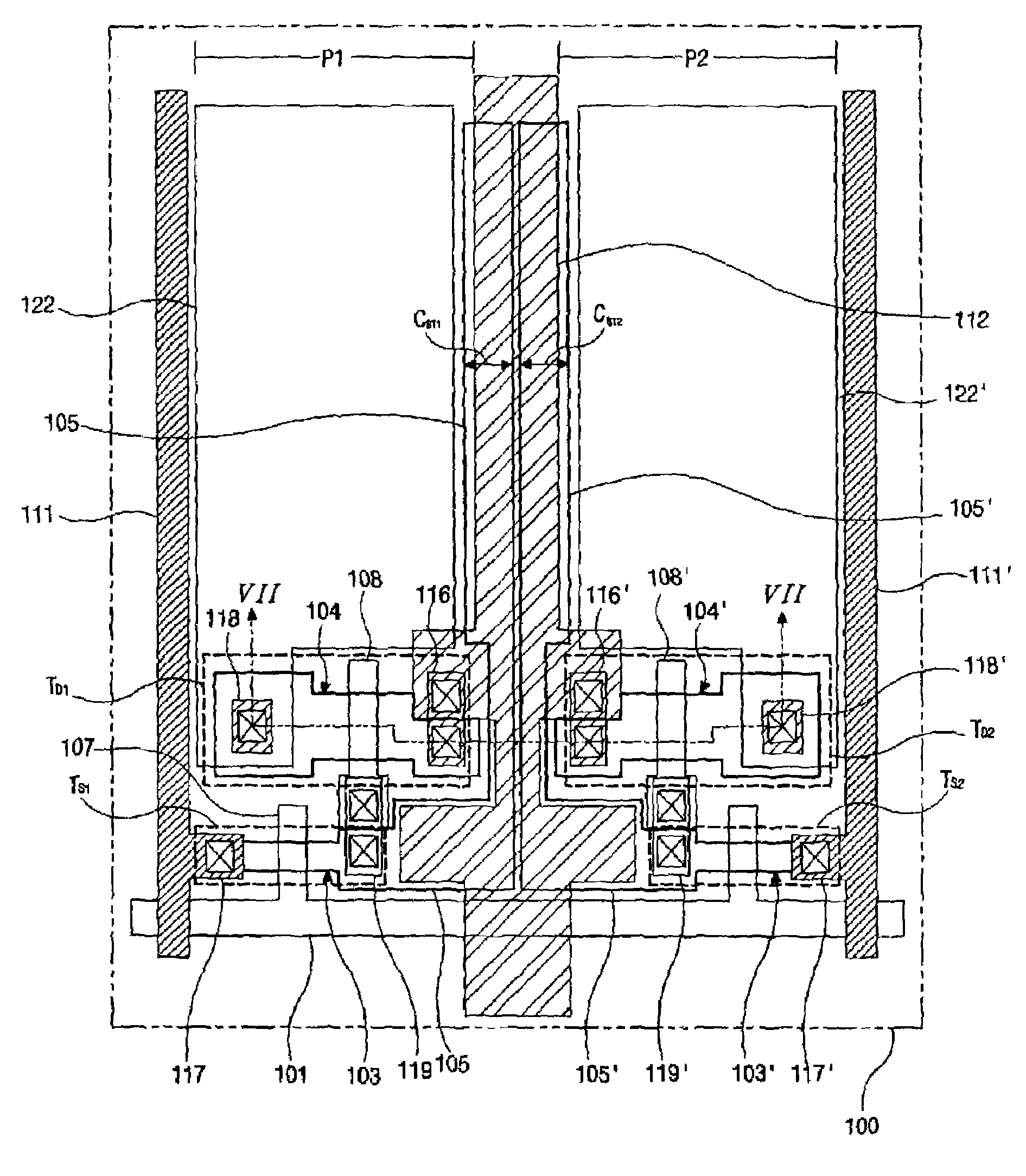
[0032]FIG. 5 is an equivalent circuit diagram of an exemplary organic electroluminescent device according to the present invention. In FIG. 5, a data line 111 may be in parallel to and separated from a power line 112. A gate line 101 may cross the data line 111 to define a pixel region P. A switching element TS, a driving element TD1, a storage capacitor CST, and an organic electroluminescent diode DEL may be formed in the pixel region P. The adjacent driving elements TD1 and TD2 of adjacent pixel regions P may be connected to the same power line 112. Since the number of the power lines 112 may be reduced by a factor of 2, the aperture ratio may increase, and the resulting device may have a resulting reduction in material cost.

[0033]FIG. 6 is a plan view of an exemplary organic electroluminescent device according to the pres...


PUM


Abstract

An organic electroluminescent device includes a substrate, a plurality of gate lines on the substrate, a plurality of data lines on the substrate, each of the plurality of data lines crossing the gate lines, a plurality of switching elements and driving elements interconnected on the substrate, and a power line disposed in parallel to the data lines on the substrate, wherein the power line is electrically connected to at least two of the plurality of driving elements.

Description

[0001]The present invention claims the benefit of the Korean Patent Application No. 2002-24551 filed in Korea on May 3, 2002, which is hereby incorporated by reference.BACKGROUND OF THE INVENTION[0002]1. Field of the Invention[0003]The present invention relates to a semiconductor device, and more particularly, to an organic electroluminescent device and a fabricating method thereof.[0004]2. Discussion of the Related Art[0005]In general, an organic electroluminescent device (ELD) emits light by injecting electrons from a cathode and holes from an anode into an emission layer, combining the electrons with the holes, generating an exciton, and transitioning the exciton from an excited state to a ground state. Contrary to a liquid crystal display (LCD) device, an additional light source is not necessary for the organic ELD to emit light because the transition of the exciton between states causes light to be emitted. Accordingly, the size and weight of the organic ELD can be reduced. The...

Claims


Application Information

Patent Timeline
Patent Type & Authority Patents(United States)
IPC IPC(8): H01J1/62H05B33/00H05B33/26G09F9/30G09G3/32H01L27/32H01L29/786H01L51/50H05B33/10H05B44/00
CPCG09G3/32H01L27/3276H01L27/3251G09G2300/0439G09G2300/0842G09G2300/08H01L27/1255H01L27/124H10K59/127H10K59/131H05B33/26
Inventor CHAE, GEE-SUNGPARK, JAE-YONGKIM, OCK-HEE
Owner LG DISPLAY CO LTD
Why Eureka
Try Eureka