Circuit and method for inducing jitter to a signal

a circuit and signal technology, applied in the field of circuits and methods for inducing jitter to signals, can solve the problems of difficult to achieve small amounts of accurate delay time, difficult to get an accurate delay time for high frequencies, and not always ideal condition of digital signals provided to digital circuitry

Inactive Publication Date: 2006-02-14
TEKTRONIX INT SALES GMBH
View PDF7 Cites 10 Cited by
  • Summary
  • Abstract
  • Description
  • Claims
  • Application Information

AI Technical Summary

Benefits of technology

[0014]The jitter inducing circuit may further have an input delay means to provide a delayed reference pulse train to the switch means. This allows the switch control means to use the input pulse as a trigger for controlling the supply of the pulses to the delay blocks. Because the delay time setting of the delay block does not change while the pulses pass through it, the order of the passing pulses do not change. Therefore, the delay block can adopt digital delay circuits that change the delay time by selectively connecting a plurality of delay elements. The digital delay circuit can provide an accurate delay time as a user desires, and then the change of the delays over time can be controlled to trace a desired function such as a sinusoidal or triangular function.
[0015]The delay block may have a buffer that provides non-inverted and inverted outputs. A first delay circuit delays the non-inverted output according to a preset delay time. A first one-shot pulse circuit converts the output of the first delay circuit into a one-shot pulse. A second delay circuit delays the inverted output according to a preset delay time. A second one-shot pulse circuit converts the output of the second delay circuit into a one-shot pulse. A logic circuit generates a first logic state in response to the output of the first one-shot pulse circuit, and generates a second logic state in response to the output of the second one-shot pulse circuit. This configuration enables the desired delay time to be set regardless of the pulse width in the reference pulse train.

Problems solved by technology

Digital signals provided to digital circuitry are not always in an ideal condition with noise in the digital signal producing jitter.
However, it is difficult for this analog method to produce a linear ramp waveform for high frequencies so it is difficult to get an accurate delay time for the high frequencies.
In addition, random jitter in the comparator makes it difficult to produce small amounts of accurate delay time.
However, this would require many ICs to generate the many kinds of pulse trains.
A digital delay circuit as shown in FIG. 3 can provide an accurate delay time, but develops problems if the delay time is changed dynamically.

Method used


Image

  • Circuit and method for inducing jitter to a signal
  • Circuit and method for inducing jitter to a signal
  • Circuit and method for inducing jitter to a signal

Examples


Embodiment Construction

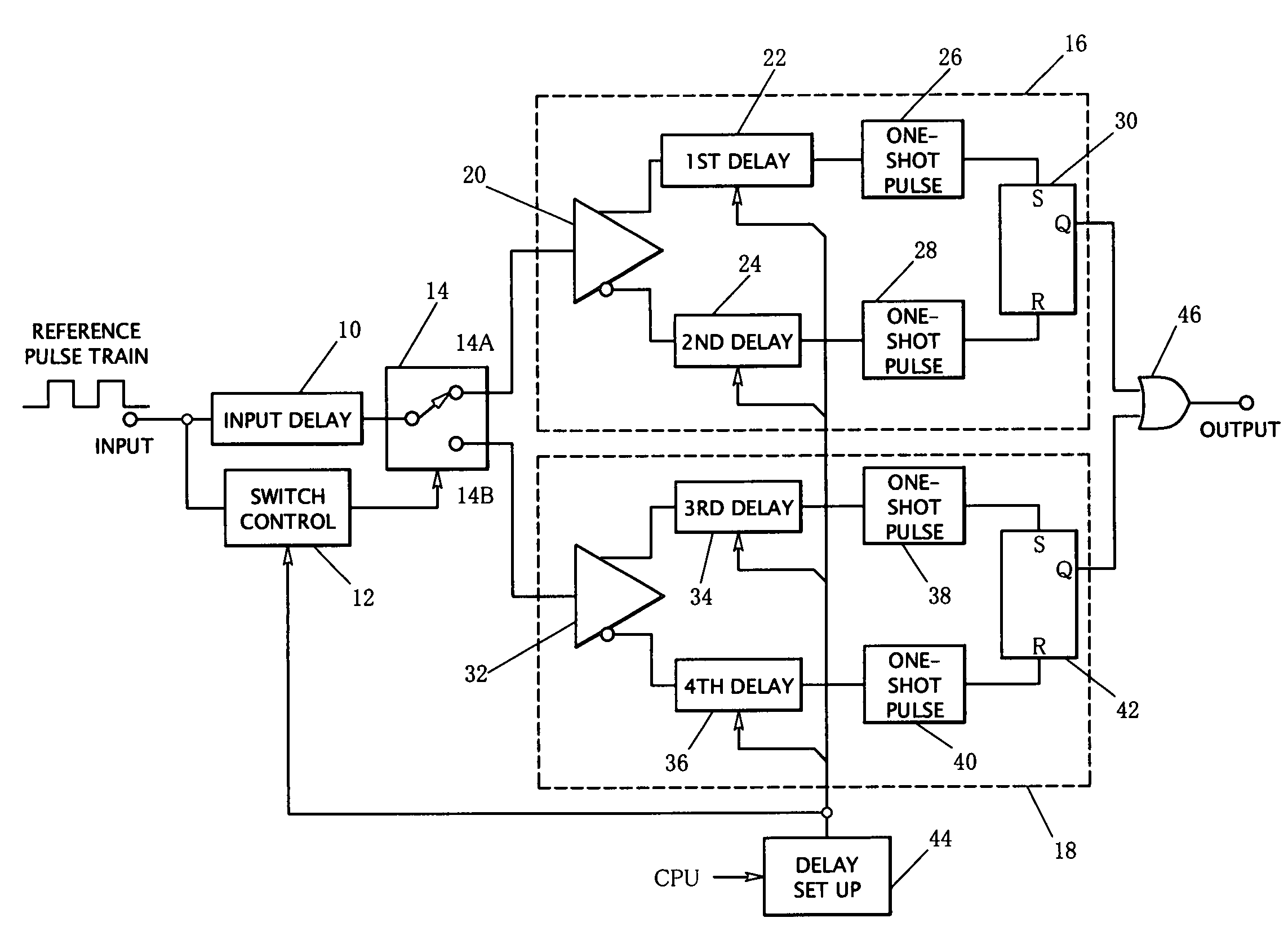
[0033]A jitter inducing circuit according to the present invention can provide fast, accurate and continuous delay times to edges of an input reference pulse train. The input pulse train may be a normal pulse train used in various digital circuits, and is called a reference pulse train hereinafter. The output pulse train of the jitter inducing circuit may serve as a jitter tolerance test signal that is used for determining how much jitter causes operational errors in a digital circuit under test.

[0034]FIG. 4 shows a schematic block diagram of a first embodiment of the jitter inducing circuit according to the present invention. The jitter inducing circuit operates under microprocessor control having well-known peripherals for a microprocessor system such as display, keyboard, mouse, CPU, RAM and hard disk drive though they are not shown. The hard disk drive stores computer program for conducting the procedures of the present invention.

[0035]An input delay circuit 10 and a switch cont...


PUM


Abstract

A jitter inducing circuit receives a reference pulse train and induces desired amounts of jitter to the rising and/or falling edges of the pulses. First and second delay blocks 16 and 18 alternately delay the selected edge or edges of the provided reference pulse train interval by preset delay times for every interval. A signal composer 46 composes the outputs of the first and second delay blocks 16 and 18. A delay time setup circuit controls the delay times of the delay blocks 16 and 18. The delay times may change for each interval as a function of time so as to trace a desired function such as a sinusoidal or triangular function.

Description

BACKGROUND OF THE INVENTION[0001]The present invention relates generally to jitter generators and more particularly to circuits and methods for intentionally inducing desired amounts of jitter to the edges of pulses of a pulse train for use for testing a device under test.[0002]Digital signals provided to digital circuitry are not always in an ideal condition with noise in the digital signal producing jitter. Therefore, digital circuits are required to be able to operate in the presence of jitter in the digital signal, or pulse train. It is also important to test digital circuits during development using digital test signals or pulse trains that include jitter. This test is called jitter tolerance test.[0003]A jitter test signal may be generated by inducing jitter to a stable digital test signal, called a reference pulse train hereafter. The reference pulse train and the jitter pulse train are provided to a digital circuit and would allow for a comparison test between the stable ref...

Claims


Application Information

Patent Timeline
Patent Type & Authority Patents(United States)
IPC IPC(8): H03K5/12H03K5/156G01R29/26H03K5/159
CPCH03K5/159G01R29/26
Inventor TAKAHASHI, HISAOOMIYA, FUJIHIKOOKUDA, HIDEAKISAKAI, RYOICHITAKAI, TORU
Owner TEKTRONIX INT SALES GMBH
Why Eureka
Try Eureka