Delay-time correction circuit, semiconductor-device drive circuit, and semiconductor device

a technology of delay-time correction and drive circuit, which is applied in the direction of electronic switching, power conversion systems, pulse techniques, etc., can solve the problems of undesirable short circuit, distorted waveform, timing lag in switching operations between semiconductor switching elements, etc., and achieve accurate correction of deviation in output signal width. , the effect of simple configuration

Active Publication Date: 2019-08-06
MITSUBISHI ELECTRIC CORP
View PDF6 Cites 2 Cited by
  • Summary
  • Abstract
  • Description
  • Claims
  • Application Information

AI Technical Summary

Benefits of technology

[0010]The present invention is made to solve the above problem. It is an object of the present invention to provide a delay-time correction circuit, a semiconductor-device drive circuit, and a semiconductor device that are capable of, by using a relatively simple configuration, accurately correcting a deviation in the width of an output signal that is obtained from a semiconductor switching element, from the width of an input signal, where such a deviation is caused by variations in a period for a transition change of the semiconductor switching element.
[0012]According to the aspect of the present invention, when the semiconductor switching element repeating the turn-on and turn-off operations alternately is driven, in accordance with a variation in a period for a transition change in one of the turn-on and turn-off operations, a delay time during the immediately following operation, which is the other of the turn-on and turn-off operations, is corrected. Consequently, correction is made in accordance with the variation in the period for the transition change without the need for complicated analysis of the transition change and complicated adjustment in accordance with the result of the analysis. This enables the deviation in the width of the output signal of the semiconductor switching element from the width of the input signal, which is caused by the variation in the period for the transition change, to be accurately corrected with a relatively simple configuration.

Problems solved by technology

In the inverter, a semiconductor switching element that is inappropriately turned on may result in an undesirable short-circuit.
In this case, a difference in characteristic of the semiconductor switching elements or of electronic components used in the drive circuits for the semiconductor switching elements may cause a timing lag in switching operations between the semiconductor switching elements.
The difference between the widths of the signals can cause a distortion of a waveform, particularly in an inverter that generates a sine wave.
This setting typically requires complicated control.
The complicated control commonly requires a complicated configuration such as a microcomputer.
Such a configuration is difficult to be integrated within the drive circuit.
Hence, it is difficult to make an accurate, fine adjustment corresponding to the above difference between the widths of the signals.

Method used


Image

  • Delay-time correction circuit, semiconductor-device drive circuit, and semiconductor device
  • Delay-time correction circuit, semiconductor-device drive circuit, and semiconductor device
  • Delay-time correction circuit, semiconductor-device drive circuit, and semiconductor device

Examples


first preferred embodiment

[0026](Summary)

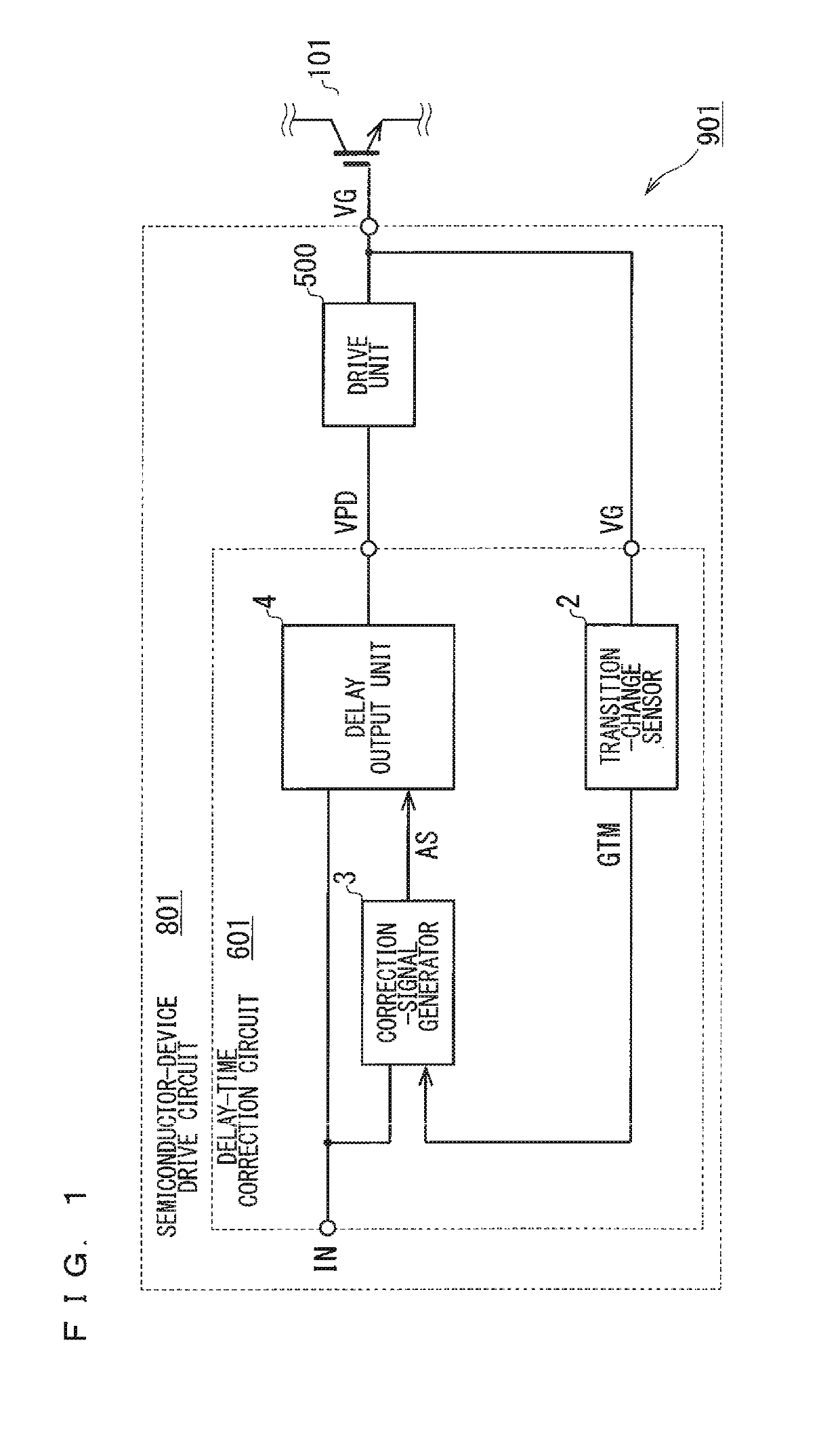
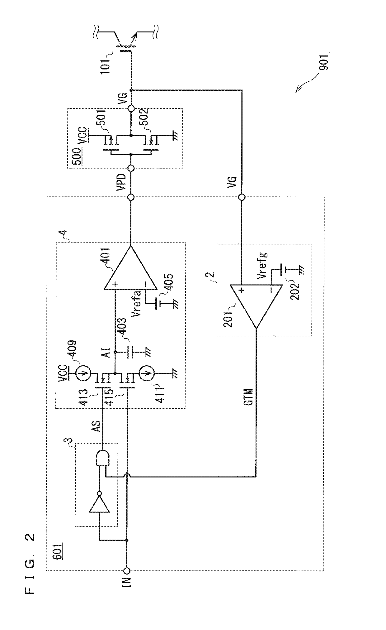
[0027]FIG. 1 is a schematic block diagram of a configuration of an inverter 901 (semiconductor device) in a first preferred embodiment. The inverter 901 includes a semiconductor-device drive circuit 801 and an IGBT 101 (semiconductor switching element). The inverter 901 performs a switching operation using a drive signal that is generated in response to an external input signal, IN. The input signal IN is a digital signal corresponding to a turn-on state and turn-off state of the IGBT 101, and is a binary signal representing a high level or low level. The drive signal is specifically a gate signal, VG, (drive signal, gate voltage) that is applied to a gate of the IGBT 101.

[0028]The semiconductor-device drive circuit 801 includes a drive unit 500 and a delay-time correction circuit 601. The delay-time correction circuit 601 may be integrated within a single integrated circuit (IC) excluding a drive unit 500. Alternatively, the delay-time correction circuit 601 may be i...

second preferred embodiment

[0066](Summary)

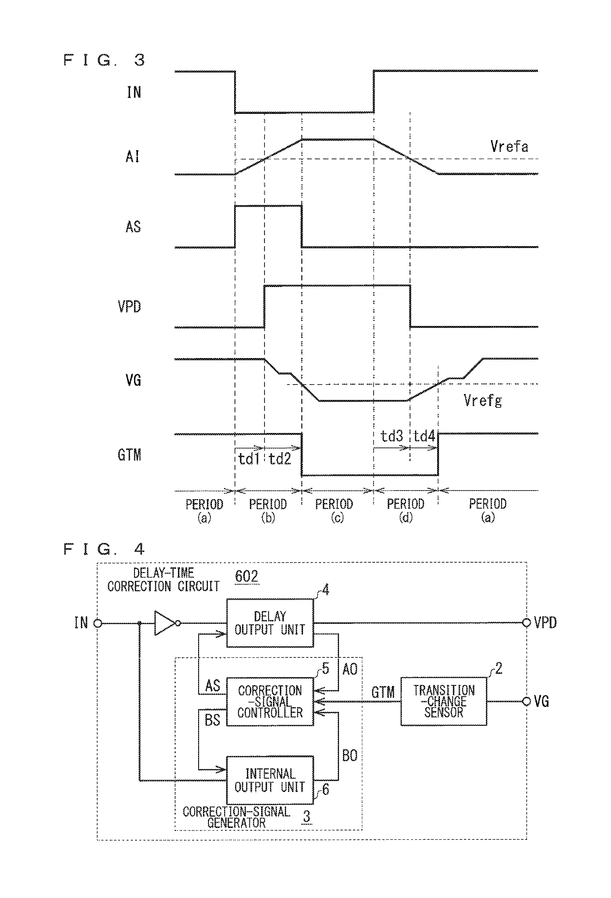
[0067]FIG. 4 is a schematic block diagram of a configuration of a delay-time correction circuit 602 in a second preferred embodiment. The delay-time correction circuit 602 can be used in the semiconductor device 901 (FIG. 1) as the alternative to the delay-time correction circuit 601. Delay-time correction circuits in the other preferred embodiments, details of which will be described later on, can be used in the same manner.

[0068]The first preferred embodiment details a configuration in which the delay output unit 4 stores the time corresponding to the length of the period for the transition change in the immediately preceding turn-off operation. The second preferred embodiment details a configuration in which the delay output unit 4 stores a time corresponding to the length of the period for the transition change in the immediately preceding turn-on operation. To conform to this configuration, FIG. 4 illustrates a NOT circuit inserted between a terminal for the inpu...

third preferred embodiment

[0095]FIG. 7 is a circuit diagram illustrating a non-limiting example of how a delay-time correction circuit 603 in a third preferred embodiment is implemented. In the third preferred embodiment, the delay-time correction circuit 603 includes a delay output unit 4c and an internal output unit 6c in place of the delay output unit 4 and internal output unit 6 in the delay-time correction circuit 602 (FIG. 5), respectively. The delay output unit 4c includes a clamp circuit incorporated into the delay output unit 4. The internal output unit 6c includes a clamp circuit incorporated into the internal output unit 6. The following described a specific configuration.

[0096]The delay output unit 4c includes a clamp circuit 417 at a positive input terminal of the comparator 401. The internal output unit 6c includes a clamp circuit 417b at a positive input terminal of the comparator 401b. The clamp circuits 417 and 417b respectively clamps the terminal voltages AI and BI during the discharge at ...


PUM


Abstract

A delay-time correction circuit delays an input signal for generating a pre-drive signal to a drive unit generating a drive signal. A transition-change sensor senses a transition change in one of a turn-on operation and turn-off operation. A correction-signal generator generates a correction signal in response to the transition change sensed by the transition-change sensor and to the input signal. A delay output unit generates an output signal corresponding to the pre-drive signal by delaying the input signal using the correction signal. The delay output unit delays the output signal that instructs the other of a turn-on operation and turn-off operation, from the input signal, in accordance with a length of a period for the transition change in the one of a turn-on operation and turn-off operation that is performed immediately before the other of a turn-on operation and turn-off operation.

Description

BACKGROUND OF THE INVENTIONField of the Invention[0001]The present invention relates to delay-time correction circuits, semiconductor-device drive circuits, and semiconductor devices. Specifically, the present invention relates to a semiconductor device with a semiconductor switching element, a semiconductor-device drive circuit for the semiconductor device, and a delay-time correction circuit for the semiconductor-device drive circuit.Description of the Background Art[0002]Inverters, which generate outputs, such as sign waves in response to signals that are externally input, include semiconductor switching elements and drive circuits. The semiconductor switching element is driven by a drive signal that is generated by the drive circuit. The drive signal is typically a gate signal that controls a gate voltage of, for example, an insulated gate bipolar transistor (IGBT) or a metal oxide semiconductor filed effect transistor (MOSFET). The drive signal is also a pulse signal generated ...

Claims


Application Information

Patent Timeline
Patent Type & Authority Patents(United States)
IPC IPC(8): H03K17/284H03K17/18H03K17/08H02H3/247H02M1/08H03K17/22H02M1/38H03K17/16
CPCH03K17/284H02H3/247H02M1/08H03K17/223H03K17/08H03K17/162H03K17/18H02M1/38H02M7/48
Inventor HOKAZONO, KAZUYAYAMAMOTO, AKIHISAWANG, DONG
Owner MITSUBISHI ELECTRIC CORP
Why Eureka
Try Eureka