[0013]In order to overcome the problems described above, preferred embodiments of the present invention provide a circuit board device and mounting method therefor having improved reliability. In the circuit board device of preferred embodiments of the present invention, even when the
land area is increased, the protruding dimension of the solder can be sufficiently secured on the land in a substrate mounting step, and the
bonding strength of the substrate to the land can be increased, thereby forming a stable connection therebetween.
[0016]According to the circuit board device described above, before the substrate is mounted on the motherboard, the solder can be applied, for example, from the end-
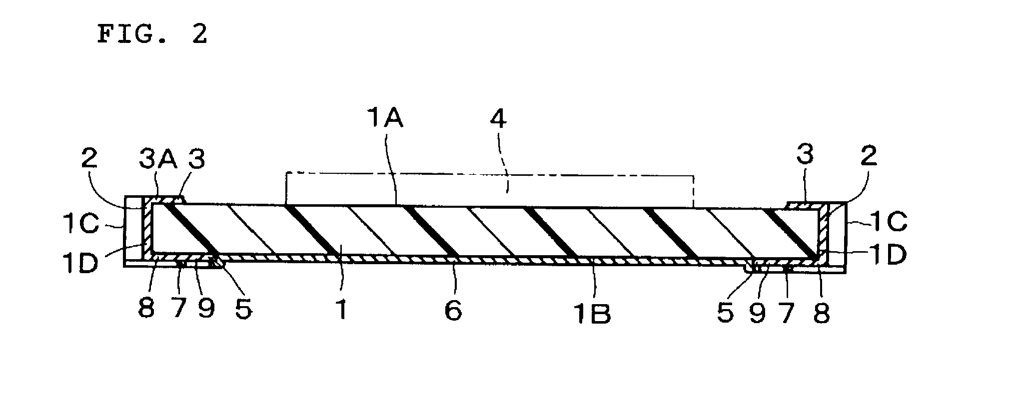
surface electrode to the mainland, and in this step, the solder melted can be prevented by the partition from flowing from the mainland into the sub-land. Accordingly, since the solder which remains on the mainland can be solidified in the state in which the solder protrudes downward by its
surface tension and its own weight, in a substrate mounting step, this protruding portion of the solder can be melted while being in contact with the motherboard, and as a result, the warping or other defect of the substrate can be ignored. In addition, the solder pushed out from between the mainland and the motherboard overflows the partition into the sub-land, and hence both the mainland and the sub-land, which have a large area, can be securely soldered to the motherboard side.
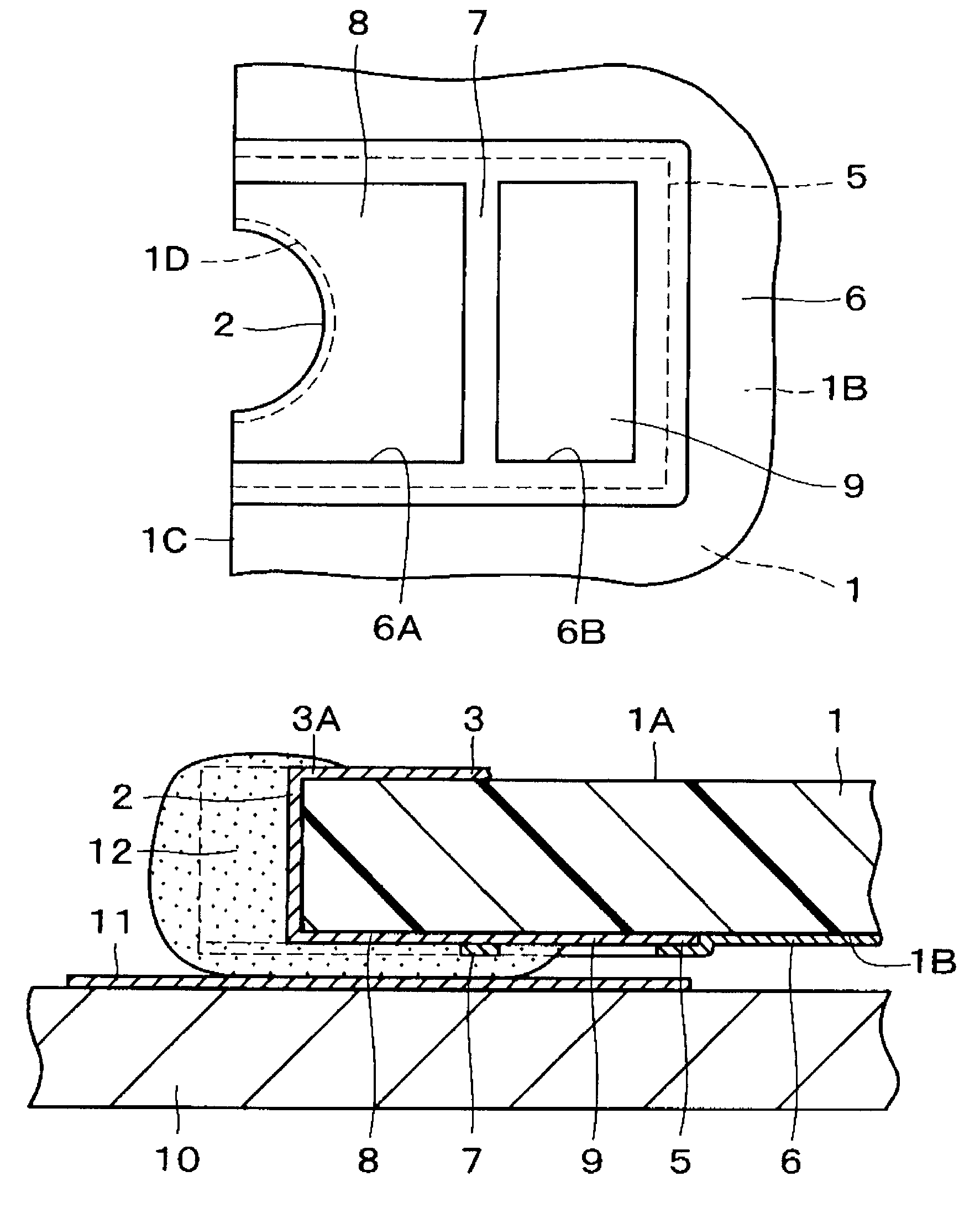
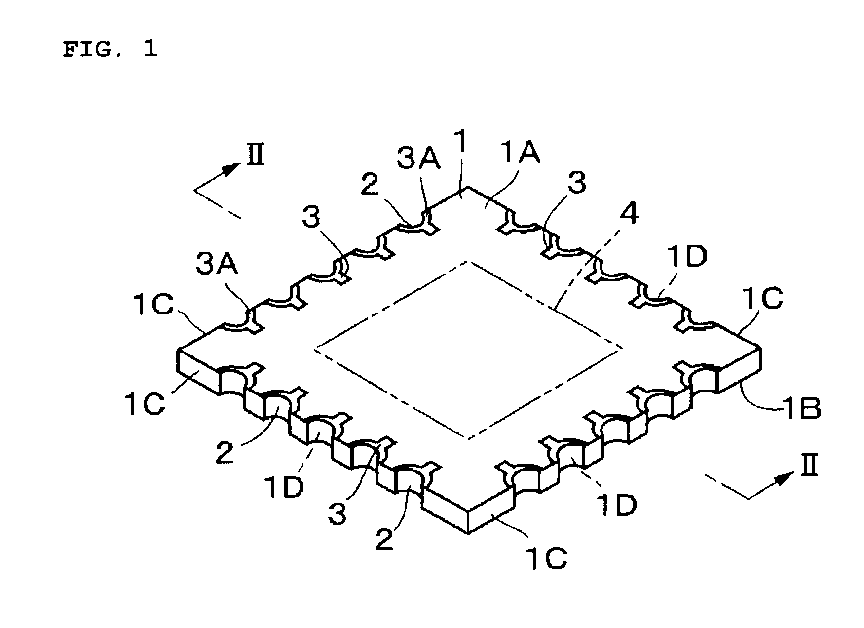
[0023]As a result, when the substrate is mounted, solder may be concentrated at the notch portion so as to promote the flow of the solder from the mainland to the sub-land, and hence the solder surely overflow the partitions. In addition, since a position through which the solder flows is limited only to the notch portion, even when the mainlands are disposed at small intervals, the solder will not flow into adjacent mainlands, and hence short-circuiting therebetween can be avoided.
[0026]Accordingly, in a step of applying solder to the substrate, only a small portion of the solder adhered to the mainland flows into each sub-land, in which the amount of the solder corresponds, for example, to the area, the width dimension, and the like of each sub-land. Hence, in the sub-land, a thin portion (expansion portion) in which the solder spreads along the sub-land can be formed. In a step of mounting the substrate on the motherboard, when being melted, the solder provided between the substrate and the motherboard is first melted and distorted, thereby bonding the mainlands to the motherboard. In addition, since each sub-land is in the state of
solder wetting as the expansion portion of the solder is melted, an excess solder distorted from between the mainland and the motherboard and pushed out therefrom can be spread smoothly along each sub-land which is in the state of
solder wetting.
[0028]According to another preferred embodiment of the present invention, in a circuit board device, there are provided lands each having one of a substantially circular shape or a substantially oval shape in which the substantially circular arc portion thereof is larger than that having a central angle of 180°. Accordingly, compared to lands having shapes other than that described above, the solder can be most protruded downward. In addition, a mainland having a large area can be formed, and the protruding dimension of the solder can also be easily determined in accordance with the width dimension (
diameter) or other characteristic of the mainland.
[0034]Accordingly, when the solder is applied to the substrate, of the solder adhered to the mainland, for example, a small amount of the solder corresponding to the area, width dimension, and the other portions of each sub-land flows therein. Hence, in the sub-land, the thin extending portion composed of the solder extending along the sub-land, is formed. In a step of mounting the substrate on the motherboard, when the solder is melted, the solder at the mainland side is distorted between the substrate and the motherboard, thereby connecting the mainland to the corresponding wire pattern of the motherboard. In addition, each sub-land is in the state of
solder wetting since the extending portion of the solder is melted, and hence excess solder distorted between the mainland and the motherboard and pushed out from therebetween can extend smoothly along each sub-land. As a result, both the mainland and the sub-lands, having a large area, can be soldered to the corresponding wire pattern of the motherboard.

