Photomask having a transparency-adjusting layer, method of manufacturing the photomask, and exposure method using the photomask

a technology of transparency adjustment and exposure method, which is applied in the field of exposure apparatus, can solve the problems of reducing the design rules for manufacturing these devices, serious obstacles to manufacturing semiconductor devices with high integrated circuit patterns, and limit the resolution of the exposure process of photolithography, so as to improve the uniformity of the critical dimensions of the pattern formed on the wafer by the second exposure process

Active Publication Date: 2006-02-21
SAMSUNG ELECTRONICS CO LTD
View PDF5 Cites 47 Cited by
  • Summary
  • Abstract
  • Description
  • Claims
  • Application Information

AI Technical Summary

Benefits of technology

[0023]Accordingly, the uniformity of the critical dimensions of the pattern formed on a wafer by the second exposure process is improved, in comparison with that whi

Problems solved by technology

Moreover, the design rules for manufacturing these devices are constantly decreasing to meet the demand for semiconductor devices having higher integration densities.
However, limits in the resolution of the exposure process of photolithography pose serious obstacles to manufacturing semiconductor devices having highly integrated circuit patterns.
In particular, the uniformity that can be attained in the dimensions of the pattern formed on the wafe

Method used


Image

  • Photomask having a transparency-adjusting layer, method of manufacturing the photomask, and exposure method using the photomask
  • Photomask having a transparency-adjusting layer, method of manufacturing the photomask, and exposure method using the photomask
  • Photomask having a transparency-adjusting layer, method of manufacturing the photomask, and exposure method using the photomask

Examples


first embodiment

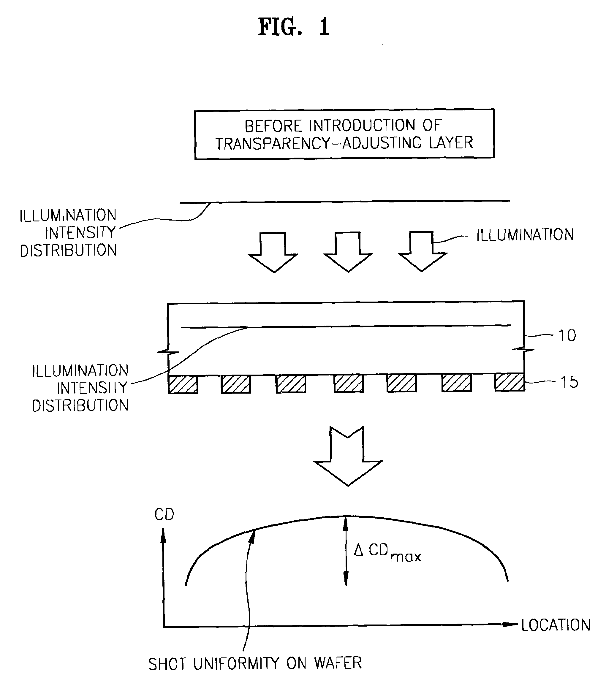
[0066]FIG. 7 illustrates the results of measuring critical dimensions of a pattern formed on a wafer through a typical exposure process before the process is corrected according to the present invention. In particular, FIG. 7 shows the magnitudes and distribution of critical dimensions of a pattern formed on a wafer through an exposure process using a conventional photomask having a design rule of 0.146 μm. The results of the measurements are shown in 5-nm wide groups ranging from 125–130 nm to 165–170 nm. The average of the critical dimensions is 148.1 nm, 3σ of the distribution of the critical dimensions is 28.8 nm, and the range of the distribution of the critical dimensions is 43.1 nm.

[0067]The critical dimensions become greater closer to the bottom of the distribution shown in FIG. 7. In other words, FIG. 7 shows that the measured critical dimensions become greater in a direction from the top to the bottom of the distribution. FIG. 8 illustrates representative doses of exposure...

second embodiment

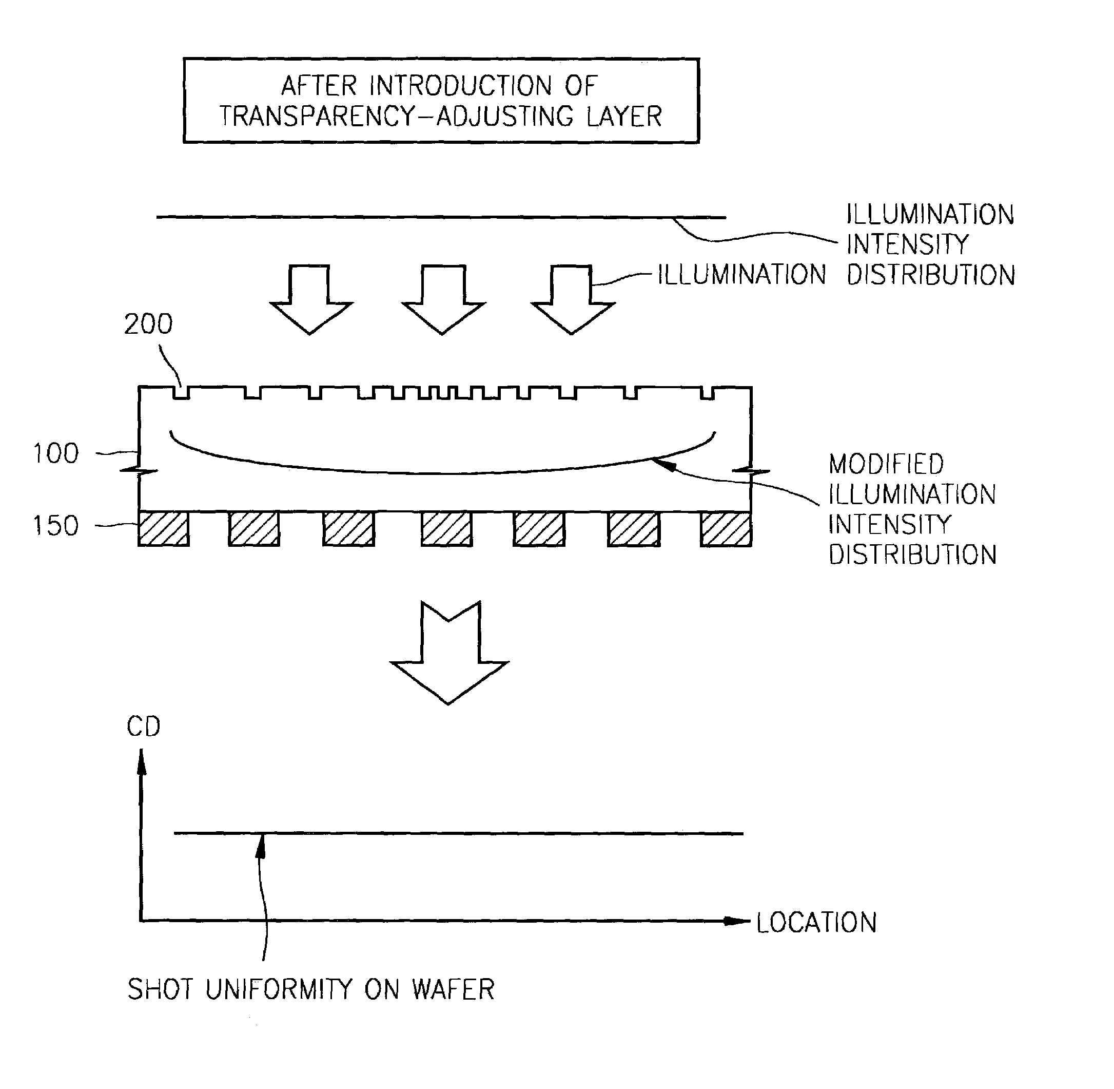
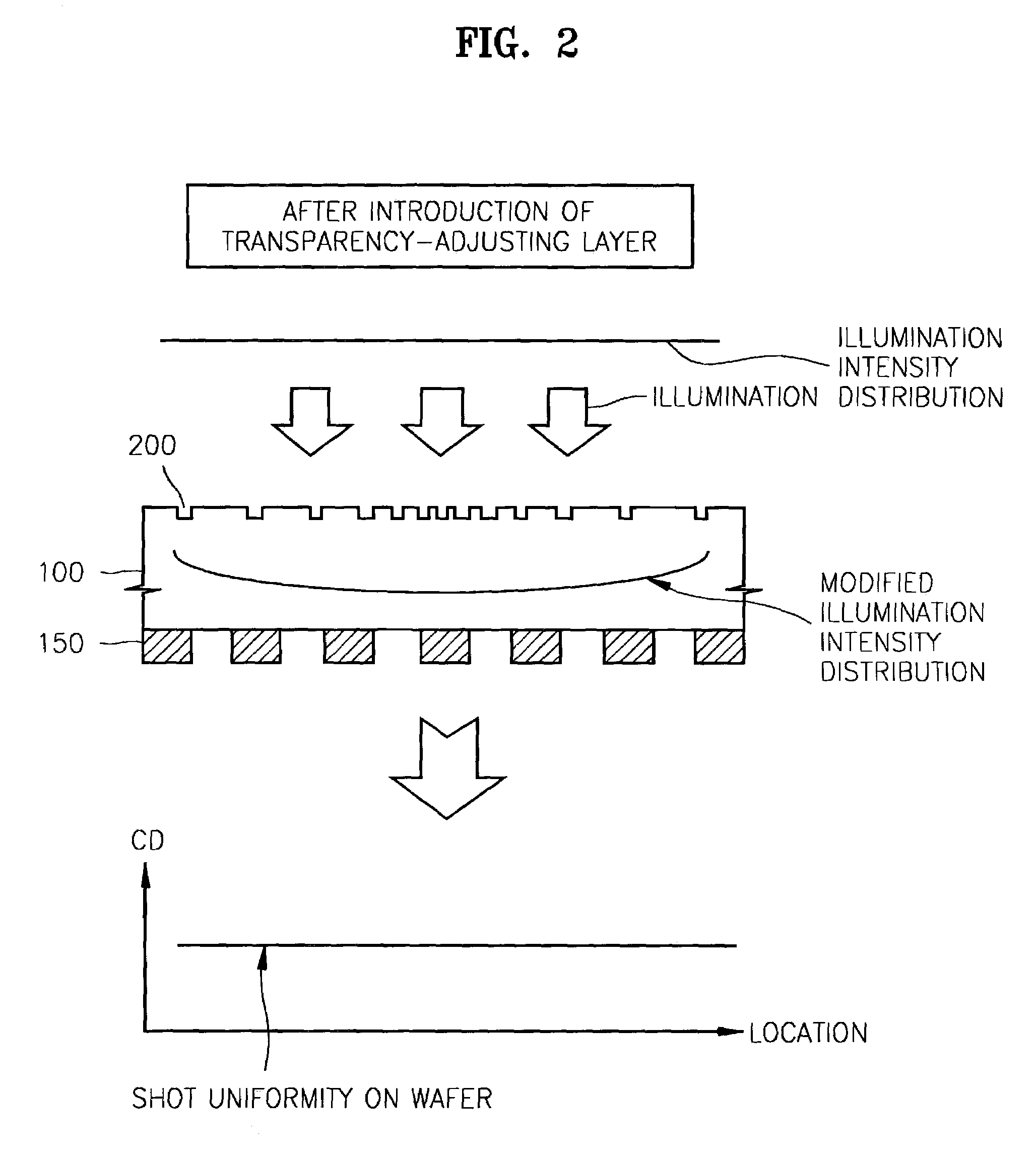
[0093]In the second embodiment of the present invention shown in FIG. 15, the transparency-adjusting pattern layer is in the form of a patterned layer of material formed on a rear side of a photomask substrate.

[0094]More specifically, a shielding layer is formed on a rear side of a photomask substrate 100. The photomask substrate 100 is a transparent substrate, for example, a quartz substrate, bearing a main pattern 150 that is to be transferred to a wafer. The shielding layer may be formed of a material, such as chromium (Cr), that can either reflect light or can absorb the light. The shielding layer is patterned thus forming transparency-adjusting pattern features 250.

[0095]The transparency-adjusting pattern features 250 reduce the intensity of light incident on the main patterns 150 by reflecting or absorbing the light incident on the rear side of the photomask. Accordingly, the transparency-adjusting pattern features 250 produce an exposure dose distribution across the wafer, si...

third embodiment

[0097]The first and second embodiments of the present invention entail photomasks wherein transparency-adjusting pattern features are provided at the rear side of the substrate of the photomask. In the third embodiment of the present invention, an auxiliary mask substrate 275 having transparency-adjusting pattern features 270 is attached to the rear side of a photomask substrate, as shown in FIG. 16.

[0098]The photomask substrate 100 is a transparent substrate, for example, a crystalline substrate. As was described above, the main pattern 150 to be transferred to a wafer is formed on the front side of the photomask substrate 100. The auxiliary mask substrate 275 may be bonded to the photomask substrate 100, at the rear side of the photomask substrate 100, by bonding material 279.

[0099]The transparency-adjusting pattern features 270 are recesses formed in the rear side of the auxiliary mask substrate 275. In this case, light passing through the recesses is out of phase with respect to...


PUM


Abstract

A photomask for use in photolithography has substrate, a main pattern at one side of the substrate, and a transparency-adjusting layer at the other side of the substrate. The transparency-adjusting layer has a characteristic that allows it to change the intensity of the illumination incident on the main pattern during the exposure process accordingly. In manufacturing the photomask, a first exposure process is carried out on a wafer using just the substrate and main pattern. The critical dimensions of elements of the pattern formed on the wafer as a result of the first exposure process are measured. Differences between these critical dimensions and a reference critical dimension are then used in designing a layout of the transparency-adjusting layer in which the characteristic of the layer is varied to compensate for such differences.

Description

BACKGROUND OF THE INVENTION[0001]1. Field of the Invention[0002]The present invention relates to the process of photolithography used to manufacture semiconductor devices. More particularly, the present invention relates to a photomask of an exposure apparatus of photolithographic equipment, and to a method of manufacturing the photomask.[0003]2. Description of the Related Art[0004]Photolithographic techniques have been widely used, in the manufacturing of semiconductor devices, to form patterns on a wafer by transcribing a pattern of a photomask onto a wafer. In these techniques, a photoresist layer is formed on the wafer. The photoresist layer is exposed to light directed through the photomask, whereby an image corresponding to the pattern of the photomask is formed on the photoresist layer. The exposed photoresist layer is then developed, which process patterns the photoresist layer. Then, a layer(s) underlying the photoresist layer is / are etched using the patterned photoresist l...

Claims


Application Information

Patent Timeline
IPC IPC(8): G01F9/00G02B5/18G02B27/09G02B27/46G03F1/26G03F1/60G03F1/68H01L21/027
CPCG02B5/1871G02B27/09G02B27/0927G02B27/0938G03F7/70191G03F1/14G03F1/144G03F1/38G02B27/46G03F1/50H01L21/027
Inventor PARK, JONG-RAKCHOI, SEONG-WOONYEO, GI-SUNGJANG, SUNG-HOON
Owner SAMSUNG ELECTRONICS CO LTD
Why Eureka
Try Eureka