Dual port memory core cell architecture with matched bit line capacitances

a dual-port memory core cell and capacitance matching technology, applied in the direction of digital storage, instruments, semiconductor devices, etc., can solve the problems of small voltage offsets with substantial performance deterioration ramifications, hammering the speed at which sense amplification may occur, and voltage offsets that become problemati

Inactive Publication Date: 2006-02-21
ARM INC
View PDF4 Cites 20 Cited by
  • Summary
  • Abstract
  • Description
  • Claims
  • Application Information

AI Technical Summary

Benefits of technology

[0017]A core cell with an expanded layout is described herein as a preferred embodiment of the present invention. The cell is fabricated upon a three column substrate of N-type substrate, P-type substrate and N-type substrate. The core cell fabricated upon this three column substrate is reduced in height with respect to known core cells and only slightly wider than known core cells. The completed core cell is no larger in total area than known core cells and the wider but reduced height architecture allows for numerous advantages in the completed core cell.
[0018]Core cells fabricated using this preferred embodiment are reduced in overall height from known core cells, which in turn reduces the length of the bitlines running down a column of core cells. The reduced bit line height in the preferred embodiment in turn reduces the bit line capacitance, resulting in faster memory operation. The preferred embodiment also improves the internal capacitance balance as a result of improved matching of internal node capacitances permitted by the new architecture. The improved capacitance balance also improves overall memory performance.
[0019]The expanded architecture also greatly simplifies the placement and routing of the power lines and bitlines in the completed core cell. As will be shown in the detailed description of the preferred embodiments, the bitlines and their complement bitlines are separated by either ground lines or power lines. The separation of the bitlines and bitline complements eliminates capacitive coupling between these lines and also results in faster memory operation.
[0020]Core cells fabricated on a substrate fabricated according to the present invention are symmetrical in layout and can be flipped about their X and Y axis as needed to offset bitline and word line voltage mismatches. This new layout also permits vertical power lines, both VDD and ground, which improves the power grid structure and also separates the bitlines. The separate power lines also permit simplified voltage biasing to reduce transistor leakage.

Problems solved by technology

Although such offsets are typical, they were insignificant compared to the 500 millivolt voltage differential required for triggering amplification by a sense amplifier.
Unfortunately, typical voltage offsets in the range of 5 to 30 millivolts will necessarily begin to hamper the speed at which sense amplification may occur.
It is this voltage offset that becomes problematic when voltage sensing between the bitlines is required at lower voltage differentials.
Thus, even very small voltage offsets have substantial performance deteriorating ramifications.
Unfortunately, conventional memory device performance is limited by the expected fabrication imperfections and layout constraints that produce imbalances in capacitive loading of the bitlines of each core cell 12.
Although well known, dual port memory core cells laid out in the manner shown in FIG. 4 have certain performance limitations and problems.
The bitlines are also typically closer together than is optimal, resulting in charge coupling between the bitlines, which reduces the speed of the core cell.
Given the layout of known SRAM core cells, it is not possible to move the bitlines sufficiently far apart to eliminate this problem.
Capacitance matching on the various bitlines is also difficult and limited space in the core cell prevents moving bitlines around to reduce this problem.

Method used


Image

  • Dual port memory core cell architecture with matched bit line capacitances
  • Dual port memory core cell architecture with matched bit line capacitances
  • Dual port memory core cell architecture with matched bit line capacitances

Examples


Embodiment Construction

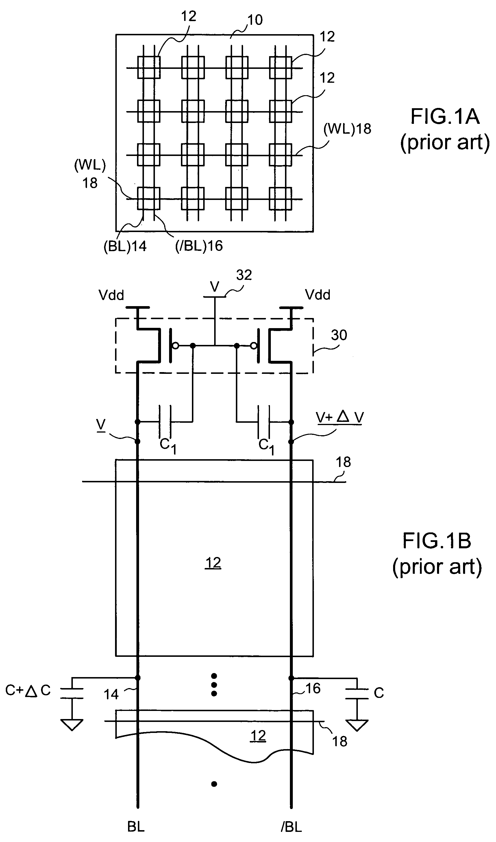
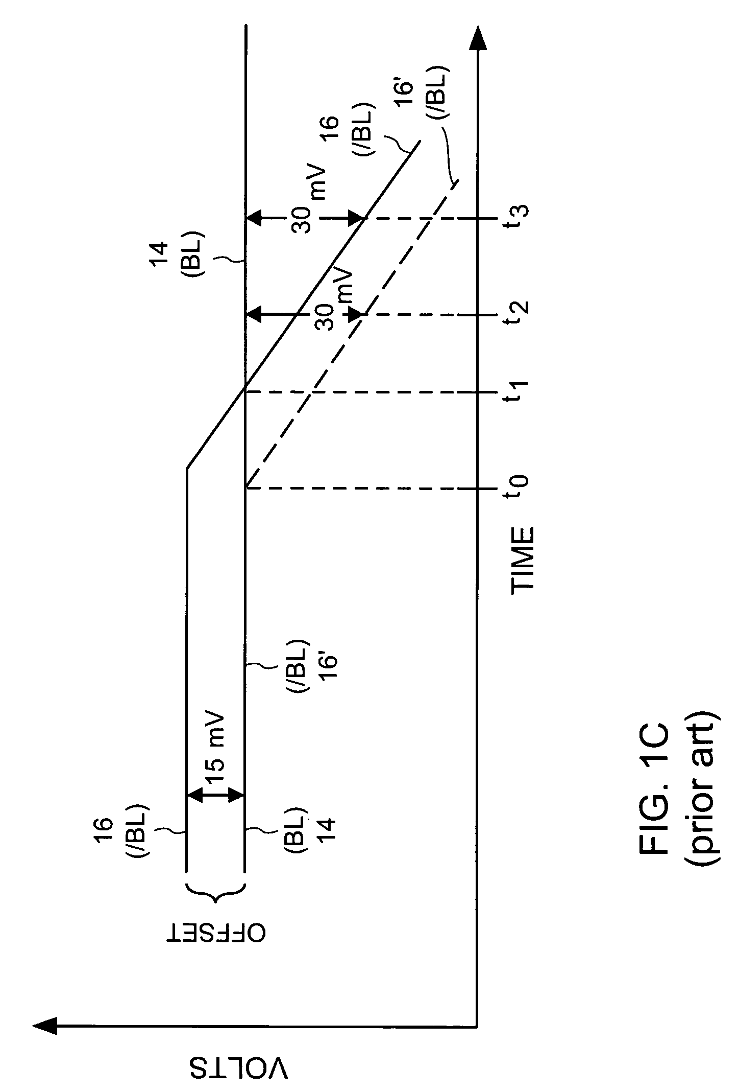
[0030]FIGS. 1a, 1b, 1c, 2, 3 and 4 have already been described and discussed as the relevant background to the present invention. They require no further discussion here.

[0031]In the following description, numerous specific details are set forth in order to provide a thorough understanding of the present invention. It will be understood, however, to one skilled in the art, that the present invention may be practiced without some or all of these specific details. In other instances, well known process operations have not been described in detail in order not to unnecessarily obscure the present invention.

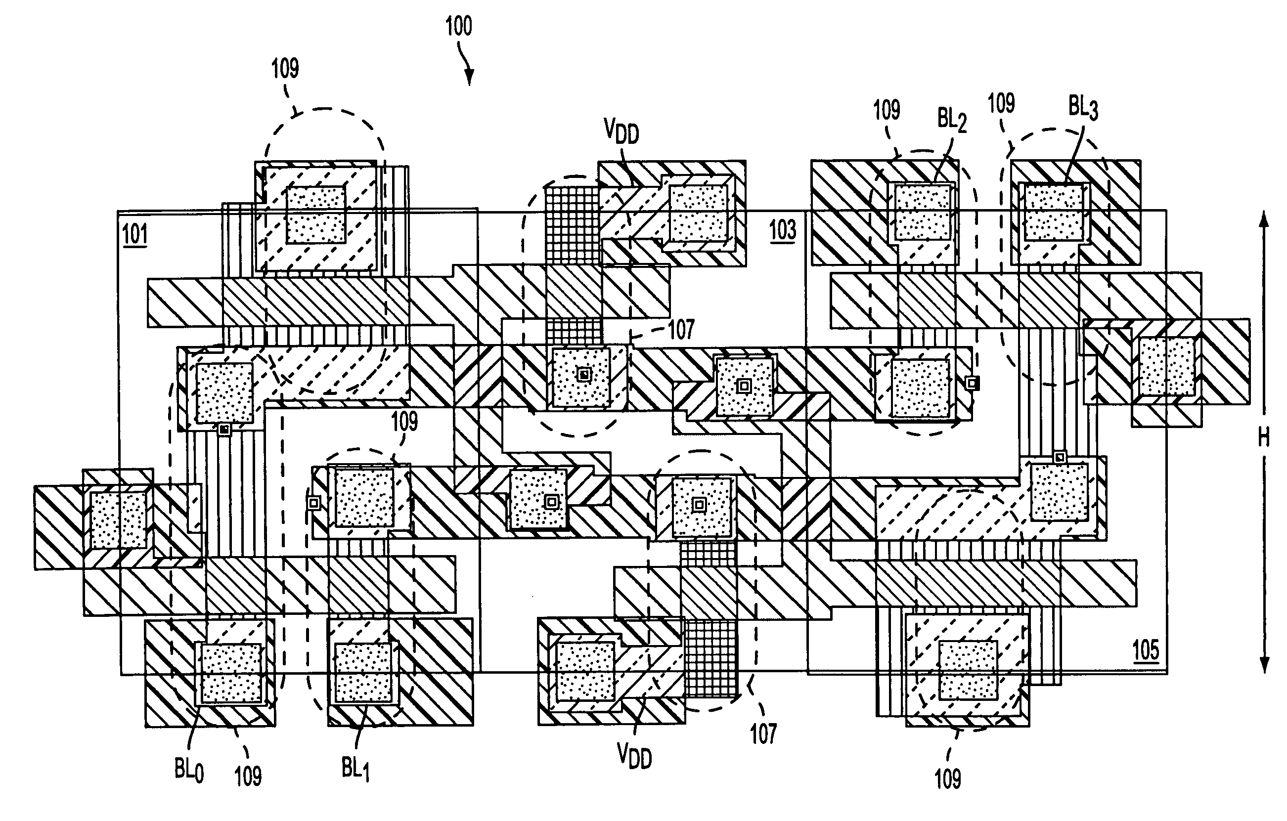
[0032]FIG. 5 illustrates the final device layout of a core cell fabricated according to the first embodiment of the present invention. Core cell 100 is fabricated upon a substrate of first p-type substrate 101, first n-type substrate 103 and second p-type substrate 105. Two pmos transistors 107 are fabricated on substrate 103 and 6 nmos transistors 109 are fabricated on substrates 10...


PUM


Abstract

A Static Random Access Memory (SRAM) dual port memory with an improved core cell design having internally matched capacitances and decreased bit line capacitance is disclosed. The core cell is fabricated on a substrate divided into three approximately equal columns of different substrate materials. In a preferred embodiment, the memory cell is fabricated on a central p-type column that in turn is sandwiched between two n-type columns. The three-column substrate architecture permits reduced bit line height, with an accompanying reduction in bit line capacitance, which increases the speed at which the core cell can operate. The architecture also permits separating the core cell's bitline and complement bitline, reducing capacitive coupling between these lines and increasing the core cell's operating speed. The architecture further permits better matching of internal node capacitances.

Description

BACKGROUND OF THE INVENTION[0001]1. Field of the Invention[0002]The present disclosure relates generally to the design and manufacture of Integrated Circuits (ICs). More specifically, the present invention relates to the design of Random Access Memory (RAM) ICs.[0003]2. Description of the Related Art[0004]Semiconductor memory is typically laid out as an array of core cells, such that each individual core cell is coupled to a wordline and a pair of differential bitlines, as well as a power and ground connection. To read or write data from or to a selected core cell requires addressing circuitry for selecting the core cell, wordline drivers for driving the selected wordline and sense amplifiers for amplifying the signals that are read from the selected core cell and output buffers.[0005]FIG. 1a is a simplified diagram of a memory 10 consisting of an array of core cells 12. Each of the core cells 12 is connected to a pair of bitlines, such as bitline (BL) 14 and a complementary bitline...

Claims


Application Information

Patent Timeline
Patent Type & Authority Patents(United States)
IPC IPC(8): H01L27/11G11C8/16G11C11/412H01L21/8244H01L27/02
CPCG11C8/16G11C11/412H01L27/0207H01L27/1104H01L27/11Y10S257/904Y10S257/903H10B10/00H10B10/12
Inventor MALI, JIMHOLD, BETINA
Owner ARM INC
Why Eureka
Try Eureka