Non-volatile semiconductor memory device with memory transistor

a semiconductor memory and transistor technology, applied in static storage, digital storage, instruments, etc., can solve the problems of excessive disadvantageous increase of threshold voltage, so as to reduce the current consumption and limit the threshold voltage of memory transistors.

Active Publication Date: 2006-02-21
RENESAS ELECTRONICS CORP
View PDF7 Cites 12 Cited by
  • Summary
  • Abstract
  • Description
  • Claims
  • Application Information

AI Technical Summary

Benefits of technology

[0007]The present invention mainly contemplates a non-volatile semiconductor memory device providing a small current consumption and a limited variation in threshold voltage of a memory transistor.
[0011]In the present non-volatile semiconductor memory device, a memory transistor's threshold voltage is detected and the resultant detection is used to set an initial value of an amplitude voltage of a pulse signal train for writing, and the pulse signal train's amplitude voltage is also increased at a rate. As compared with applying a pulse signal train of a fixed voltage regardless of a memory transistor's threshold voltage, as conventional, the present invention can achieve a reduced current consumption and a limited variation in threshold voltage of the memory transistor.
[0012]Furthermore in the present non-volatile semiconductor memory device in another aspect a pulse signal train's initial value is set to a previously determined value and a memory transistor's current value is also detected, and the resultant detection is used to set a rate applied to increase the pulse signal train's amplitude voltage and the set rate is used to increase the pulse signal train's amplitude voltage. As compared with applying a pulse signal train of a fixed voltage regardless of a memory transistor's current value, as conventional, the present invention can achieve a reduced current consumption and a limited variation in threshold voltage of the memory transistor.
[0013]Furthermore in the present non-volatile semiconductor memory device in still another aspect a fourth voltage between a memory transistor's control gate and well region is increased by a predetermined voltage stepwise and the memory transistor's current value is detected, and when the fourth voltage attains a reference voltage and the memory transistor's current value also attains a reference current, writing a data signal to the memory transistor in response stops. As compared with applying a fixed voltage between a memory transistor's control gate and well region, as conventional, the present invention can achieve a reduced current consumption and a limited variation in threshold voltage of the memory transistor.

Problems solved by technology

In conventional flash memory, however, when a memory transistor's control gate receives voltage the memory transistor has a large initial current flowing therethrough and the flash memory disadvantageously consumes a large current.
Furthermore, the memory transistor's threshold voltage is excessively increased and threshold voltage's variation is disadvantageously increased.

Method used


Image

  • Non-volatile semiconductor memory device with memory transistor
  • Non-volatile semiconductor memory device with memory transistor
  • Non-volatile semiconductor memory device with memory transistor

Examples


first embodiment

[0036

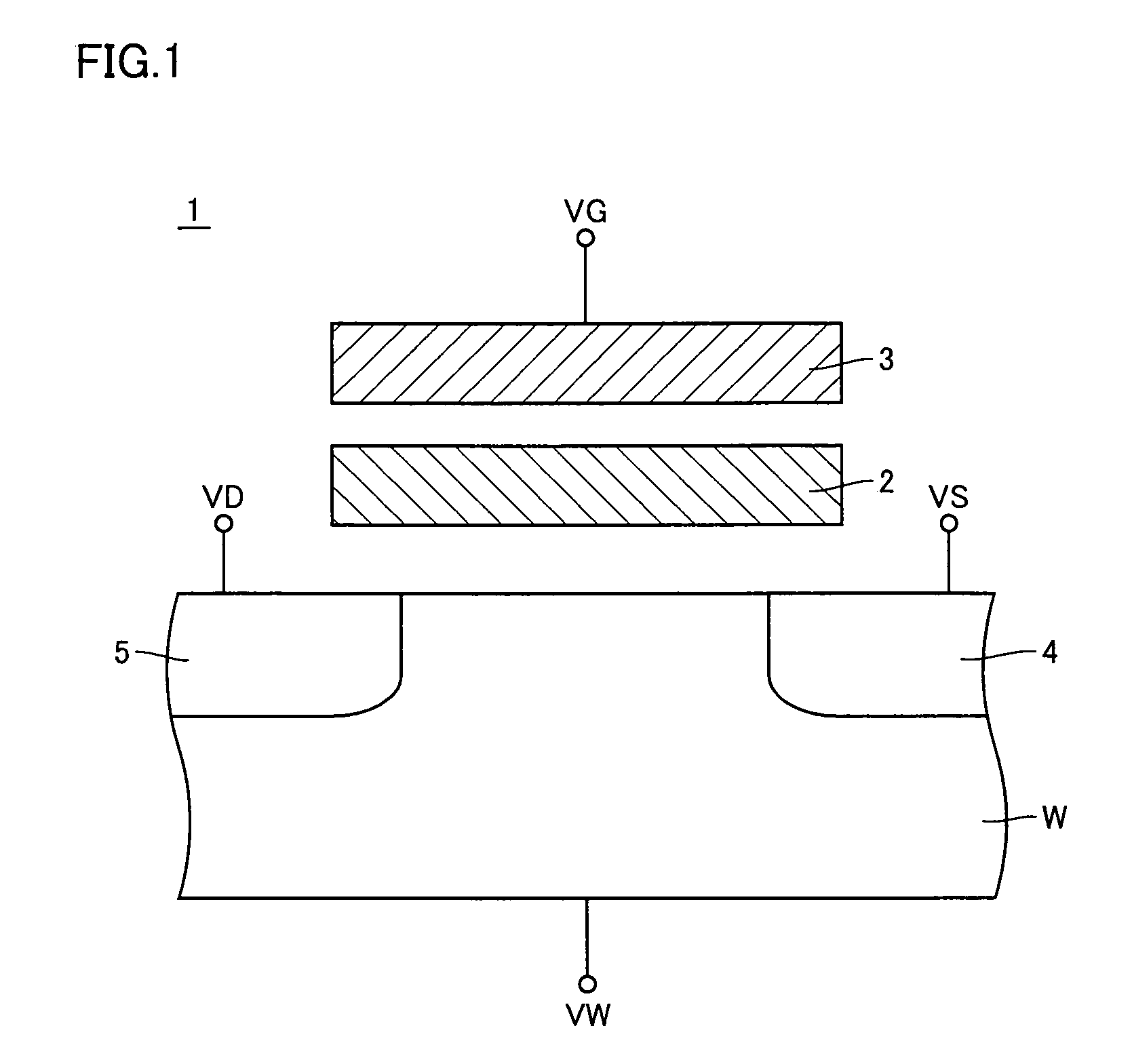
[0037]FIG. 1 is a cross section of a configuration of a memory transistor 1 of a flash memory in accordance with a first embodiment of the present invention. In FIG. 1, this memory transistor 1 includes a floating gate 2 formed above a surface of a well W at a semiconductor substrate with an insulating layer interposed, a control gate 3 formed thereabove with an insulating layer interposed, and a source 4 and a drain 5 formed on the well W surface on the opposite sides of gates 2, 3, respectively. Prescribed voltages VW, VG, VS, VD are applied to well W, control gate 3, source 4, and drain 5, respectively. Threshold voltage VT of memory transistor 1 varies depending on the number of electrons in floating gate 2.

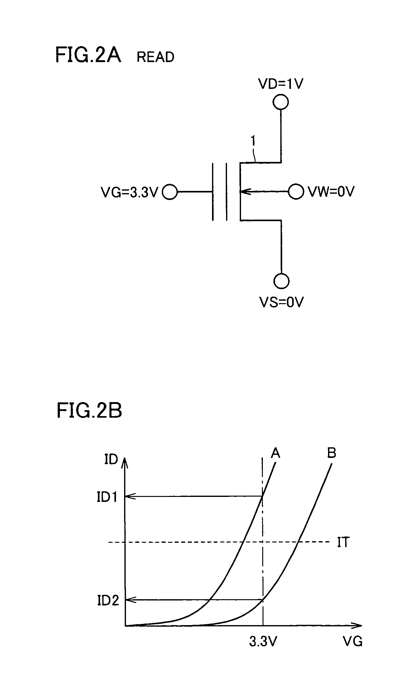
[0038]In a reading operation, as shown in FIG. 2A, 1V is applied to drain 5 of memory transistor 1, 3.3V is applied to control gate 3, and 0V is applied to source 4 and well W, so that it is determined whether a current ID between drain 5 and source 4 exceeds a prescribe...

second embodiment

[0062

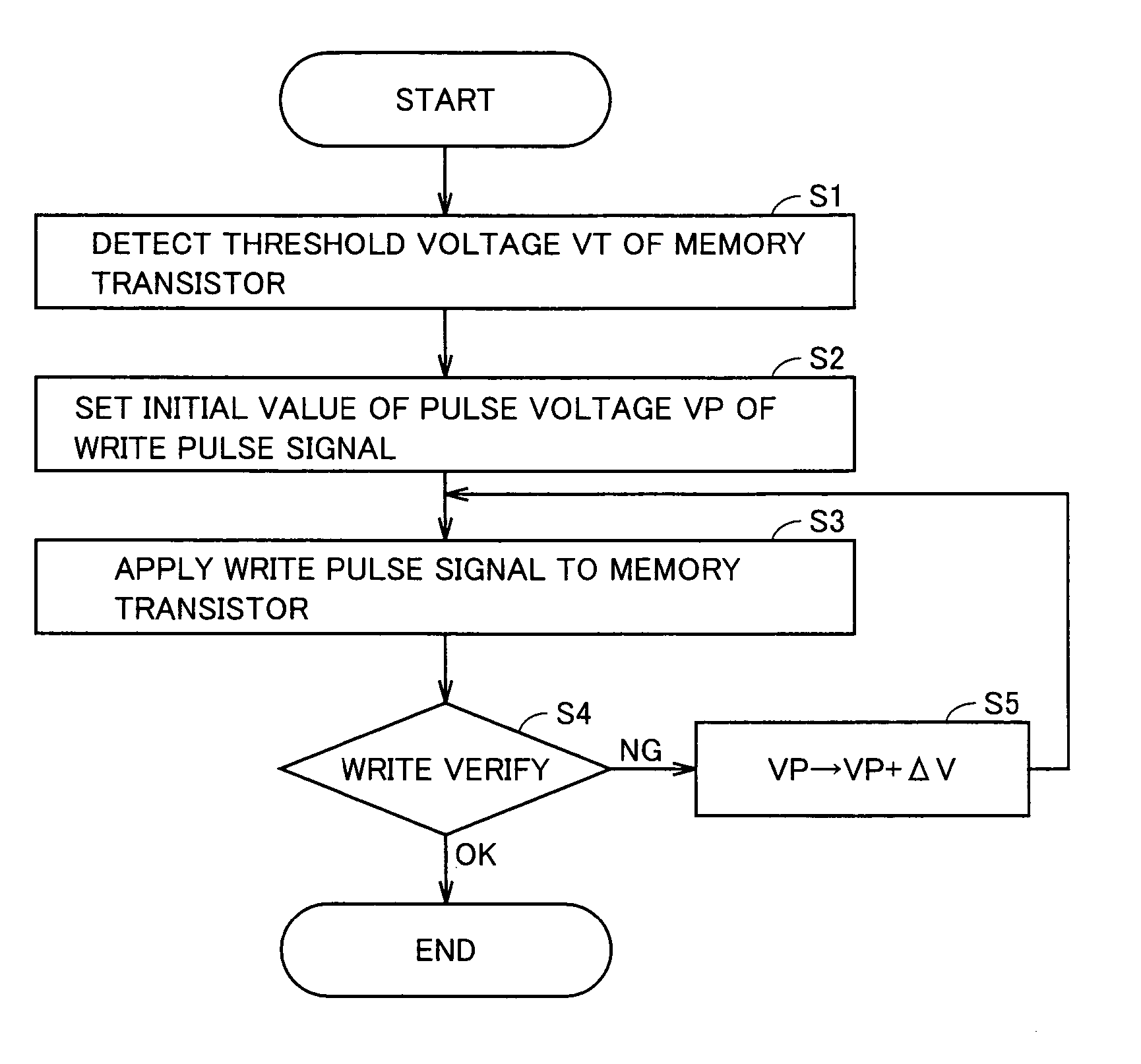
[0063]FIG. 14 is a flow chart illustrating a method employed in the present flash memory to write data in a second embodiment. With reference to FIG. 14 at step S11 threshold voltage VT of a selected memory transistor 1 is detected and at step S12 the threshold voltage VT value detected is used to set an initial value of pulse voltage VP of a write pulse signal. This process is identical to that described in the first embodiment.

[0064]Then at step S13 memory transistor 1 receives the write pulse signal and sense amplifier 15 detects the memory transistor 1 drain current ID and at step S14 verify control circuit 21 is driven by the drain current ID value detected to set step voltage ΔV. As shown in FIG. 15, the memory transistor 1 drain current ID is smaller for threshold voltage VT changing faster and is larger for threshold voltage VT changing slower. Accordingly, as shown in FIG. 16, when drain current ID is small, threshold voltage VT readily varies, and step voltage ΔV is a...

third embodiment

[0068

[0069]FIG. 18 is a circuit block diagram showing a main portion of the present flash memory in a third embodiment. FIG. 18 shows a portion associated with two data signals D1 and D2. In reality, a large number of columns are provided for a single data signal and a large number of memory transistors 1 are provided for a single column. To simplify the drawing and description, however, FIG. 18 shows a single column is shown for a single data signal and two memory transistors 1 are shown for a single column.

[0070]Two rows of memory transistors 1 are associated with word lines WL1 and WL2, respectively, and two columns of memory transistors 1 are associated with bit lines BL1 and BL2, respectively, and the four memory transistors 1 share source line SL. Memory transistor 1 has a control gate connected to the corresponding word line WL, a drain to the corresponding bit line BL, a source to the corresponding source line SL, and a back gate (well W) receiving a well voltage VW.

[0071]Wo...


PUM


Abstract

In the present flash memory a threshold voltage of a memory transistor to which data is written is detected and the detected value is used to set an initial value of a pulse voltage of a write pulse signal, and whenever the write pulse signal is applied, the pulse voltage is increased by a step voltage. The memory transistor's drain current and the threshold voltage's variation can be smaller than when a fixed pulse voltage is applied, as conventional.

Description

BACKGROUND OF THE INVENTION[0001]1. Field of the Invention[0002]The present invention relates generally to non-volatile semiconductor memory devices and particularly to those including a memory transistor having a floating gate.[0003]2. Description of the Background Art[0004]Conventionally, in flash memory, applying a fixed pulse voltage to a memory transistor at a control gate and making a decision as to whether the memory transistor's threshold voltage has reached a verify voltage are repeated to write a data signal.[0005]There is also a method applying a fixed voltage to a memory transistor at a control gate and detecting that the memory transistor's drain current has reached a reference current, and ending a write (see U.S. Pat. No. 5,422,842 for example).[0006]In conventional flash memory, however, when a memory transistor's control gate receives voltage the memory transistor has a large initial current flowing therethrough and the flash memory disadvantageously consumes a larg...

Claims


Application Information

Patent Timeline
Patent Type & Authority Patents(United States)
IPC IPC(8): G11C16/04G11C16/02G11C7/02
CPCG11C16/10G11C11/5628
Inventor OKIMOTO, HIROMIMIYAWAKI, YOSHIKAZUKISHIDA, SATORUAGAWA, DAISUKE
Owner RENESAS ELECTRONICS CORP
Why Eureka
Try Eureka