Method of forming through-the-wafer metal interconnect structures

a technology of through-the-wafer metal and interconnect structure, which is applied in the direction of semiconductor devices, semiconductor/solid-state device details, electrical apparatus, etc., can solve the problems of increasing the cost of the wafer, difficult to form the barrier layer, and a significant amount of time for the dry etching process to form the hole through the wafer

Active Publication Date: 2006-02-28
NAT SEMICON CORP
View PDF32 Cites 24 Cited by
  • Summary
  • Abstract
  • Description
  • Claims
  • Application Information

AI Technical Summary

Problems solved by technology

One drawback to a trench-based, through-the-wafer structure is that it is difficult to form barrier layer 114 and copper seed layer 116 with adequate step coverage when the aspect ratio exceeds approximately 4:1, i.e., the depth of the trench is more than four times the width of the trench.
One drawback with forming through-the-wafer holes using dry etching processes is that it takes a significant amount of time for a dry etching process to form a hole through the wafer.
As a result, to maintain production-level fabrication rates, additional dry etching equipment is required which, in turn, substantially increases the cost of the wafers.

Method used


Image

  • Method of forming through-the-wafer metal interconnect structures
  • Method of forming through-the-wafer metal interconnect structures
  • Method of forming through-the-wafer metal interconnect structures

Examples


Embodiment Construction

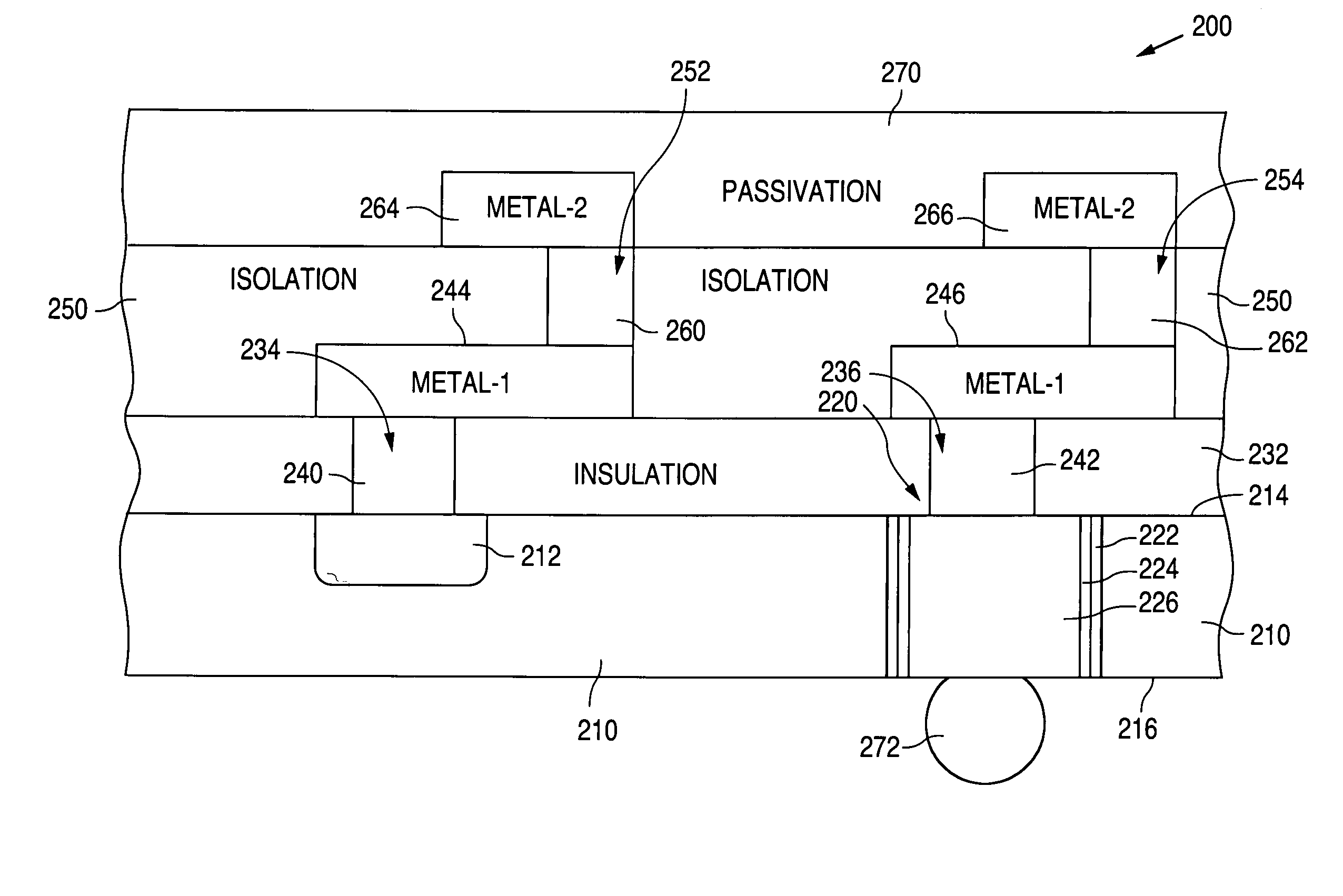
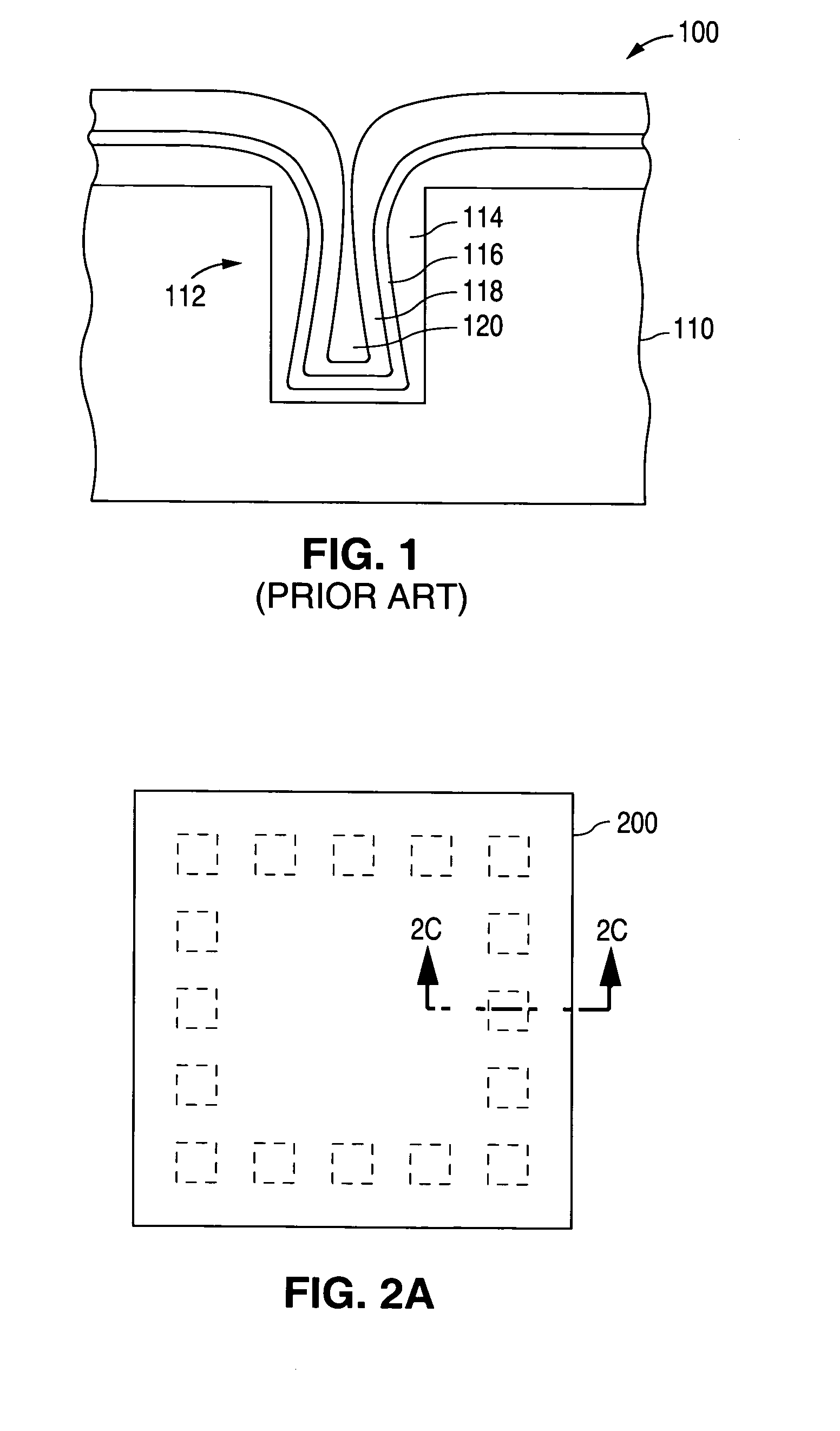
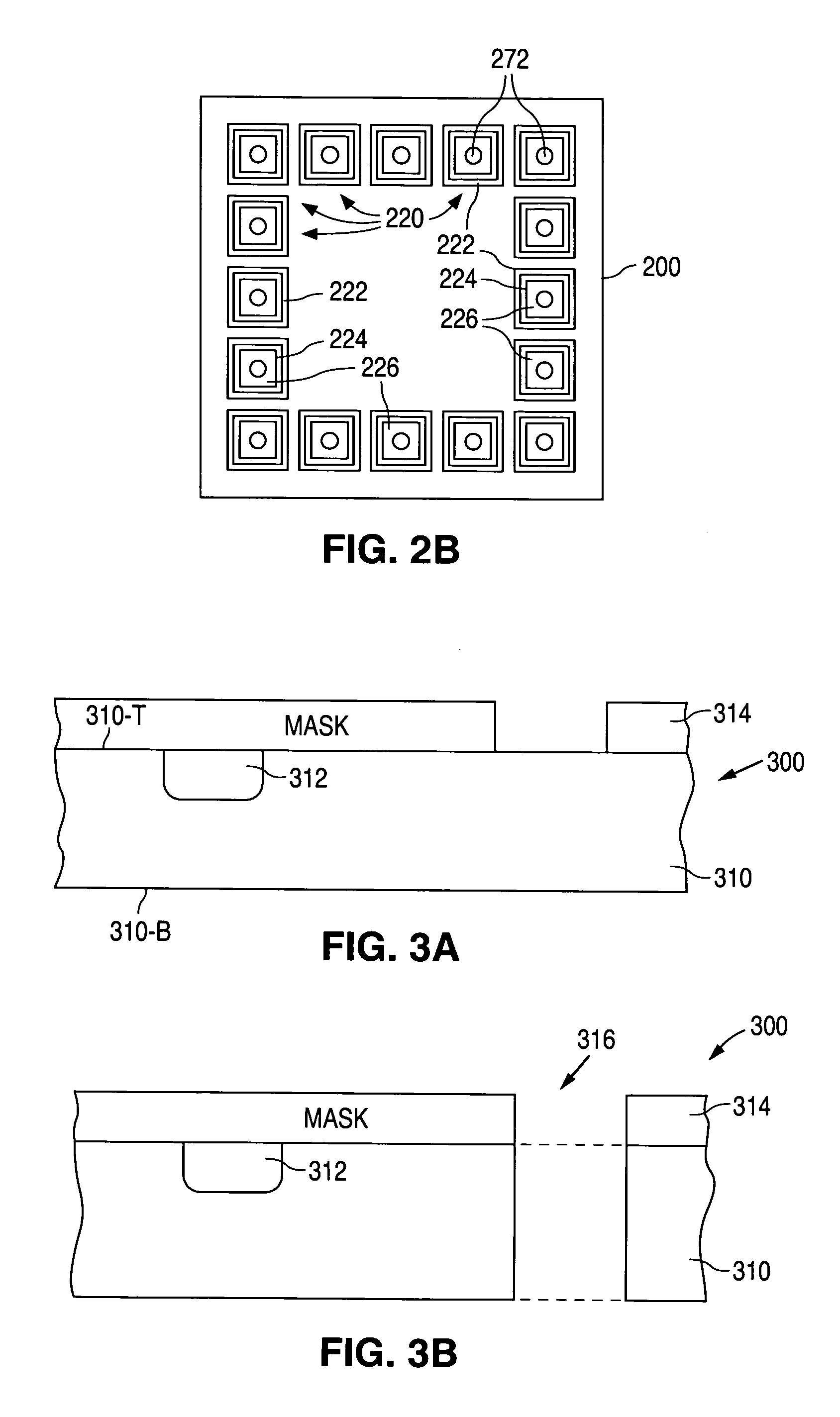
[0019]FIGS. 2A–2C show a series of views that illustrate a semiconductor die 200 in accordance with the present invention. FIG. 2A shows a plan view of semiconductor die 200, FIG. 2B shows a bottom view of semiconductor die 200, and FIG. 2C shows a cross-sectional view of semiconductor die 200 that is taken along line 2C—2C of FIG. 2A.

[0020]As shown in FIGS. 2A–2C, semiconductor die 200 includes a substrate 210, and a doped region 212 that is formed in substrate 210. Substrate 210 has a top surface 214, an opposing bottom surface 216, and a number of holes 220 that extend from top surface 214 through substrate 210 to bottom surface 216. Each of the holes 220, in turn, has substantially anisotropic side walls. Further, substrate 210 has a crystallographic orientation.

[0021]Doped region 212, which is a part of a semiconductor circuit that is formed on substrate 210, can have the same or an opposite conductivity type as substrate 210. When substrate 210 and doped region 212 share the ...


PUM


Abstract

A semiconductor die is formed in a process that forms a hole through the wafer prior to the formation of the contacts and the metal-1 layer of an interconnect structure. The through-the-wafer hole is formed by using a wafer with a <110> crystallographic orientation and a wet etch, such as with ethanol (KOH) or tetramethylammonium hydroxide (TMAH).

Description

BACKGROUND OF THE INVENTION[0001]1. Field of the Invention[0002]The present invention relates to interconnect structures and, more particularly, to a method of forming a through-the-wafer metal interconnect structure.[0003]2. Description of the Related Art[0004]An integrated circuit or chip that includes through-the-wafer metal interconnect structures can be used, for example, to electrically connect a number of integrated circuits or chips that are vertically stacked on top of each other to form a device with a substantially smaller footprint. In addition, through-the-wafer metal interconnect structures can also improve the pad layout density, and even provide backside integration opportunities.[0005]One method of forming a through-the-wafer metal interconnect structure is to first form a trench in the wafer. Once the trench has been formed, a barrier layer and a copper seed layer are subsequently formed in the trench. After the copper seed layer has been formed, a conductive metal...

Claims


Application Information

Patent Timeline
Patent Type & Authority Patents(United States)
IPC IPC(8): H01L21/302H01L21/461
CPCH01L21/76898H01L23/481H01L2224/13025H01L2224/131H01L2924/014H01L2224/05026H01L2224/0557H01L2224/05001H01L2224/05124H01L2224/05166H01L2224/05184H01L2224/05647H01L2224/05571H01L2924/00014
Inventor HOPPER, PETER J.VASHCHENKO, VLADISLAVJOHNSON, PETERDRURY, ROBERT
Owner NAT SEMICON CORP
Why Eureka
Try Eureka