Semiconductor package with photosensitive chip and fabrication method thereof

a technology of semiconductors and chips, applied in semiconductor/solid-state device details, semiconductor devices, radiation controlled devices, etc., can solve the problems of encapsulation body, reliability degradation of semiconductor packages, and undetectable drawbacks of above semiconductor packages, so as to improve the adhesion between the dam and the substrate, increase the viscosity, and improve the effect of adhesion

Inactive Publication Date: 2006-02-28
SILICONWARE PRECISION IND CO LTD
View PDF3 Cites 24 Cited by
  • Summary
  • Abstract
  • Description
  • Claims
  • Application Information

AI Technical Summary

Benefits of technology

[0006]An objective of the present invention is to provide a semiconductor package with a photosensitive chip and a fabrication method thereof, which can enhance adhesion between an encapsulation dam and a substrate on which the dam is formed, thereby preventing delamination in-between from occurrence.
[0007]Another objective of the present invention is to provide a semiconductor package with a photosensitive chip and a fabrication method thereof, which can eliminate a resin compound for forming the encapsulation dam from flashing over unintended area on the substrate, thereby assuring reliability and electrical connection of the semiconductor package.
[0010]The above semiconductor package according to the invention yields significant benefits. It is a characteristic feature that the encapsulation dam is formed on the continuous peripheral portion of the core of the substrate that is exposed via the opening of the solder mask layer, making the dam in direct contact with the core. This arrangement effectively enhances adhesion between the dam and the substrate since the dam and the core are both made of resin materials, such that delamination between the dam and the substrate can be eliminated. Moreover, the opening of the solder mask layer for exposing the peripheral portion of the core is larger in width by 0.1 to 1 mm (preferably 0.5 mm) than a cavity of a mold for forming the support portion of the dam, such that a resin compound for fabricating the dam quickly absorbs heat from the mold and increases its viscosity when flowing to the opening and approaching the edge of the solder mask layer, thereby not flashing out of the opening and over unintended area on the substrate. As a result, the chip and bonding wires would not be mounted on flash-contaminated area on the substrate, and reliability and electrical connection can be assured for the semiconductor package.

Problems solved by technology

The encapsulation body is usually opaque or non-transparent, thereby making a photosensitive chip such as CMOS (complementary metal oxide semiconductor) chip that requires light for operation not suitably incorporated in such a semiconductor package.
However, the above semiconductor package may undesirably suffer significant drawbacks.
Since adhesion between the resin compound of the encapsulation body and the solder mask is not very strong and the contact area between the encapsulation body and the substrate is relatively small, thereby delamination between the encapsulation body and the substrate may easily occur, making the reliability of the semiconductor package degrade.
Moreover, since the encapsulation body is molded onto the surface of the substrate, the resin compound may easily flash to unintended area on the substrate and contaminate bond fingers formed on the substrate during molding.
As a result, bonding wires cannot be perfectly bonded to the contaminated bond fingers, such that electrical connection between the chip and the substrate is damaged.

Method used


Image

  • Semiconductor package with photosensitive chip and fabrication method thereof
  • Semiconductor package with photosensitive chip and fabrication method thereof
  • Semiconductor package with photosensitive chip and fabrication method thereof

Examples


Embodiment Construction

[0016]The preferred embodiments of a semiconductor package with a photosensitive chip and a fabrication method thereof proposed in the present invention are described with reference to FIGS. 1, 2A–2D and 3A–3D.

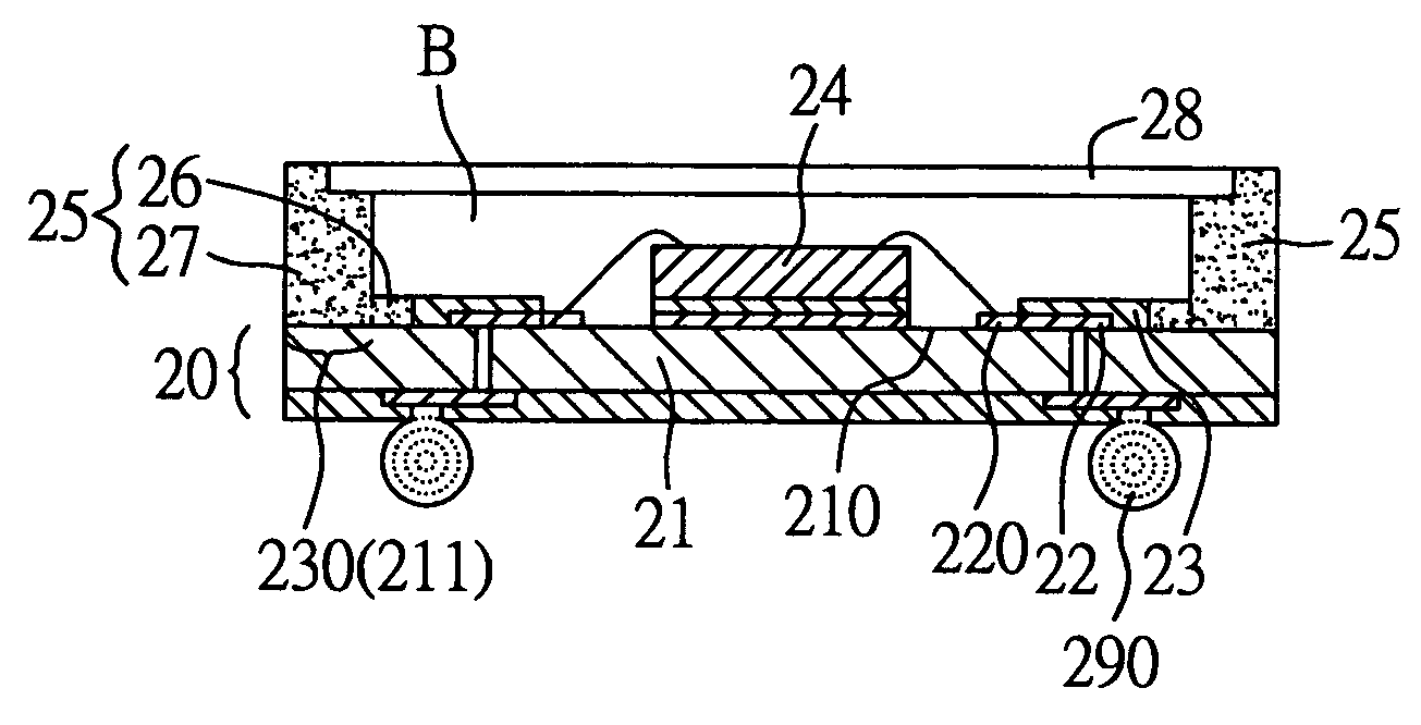
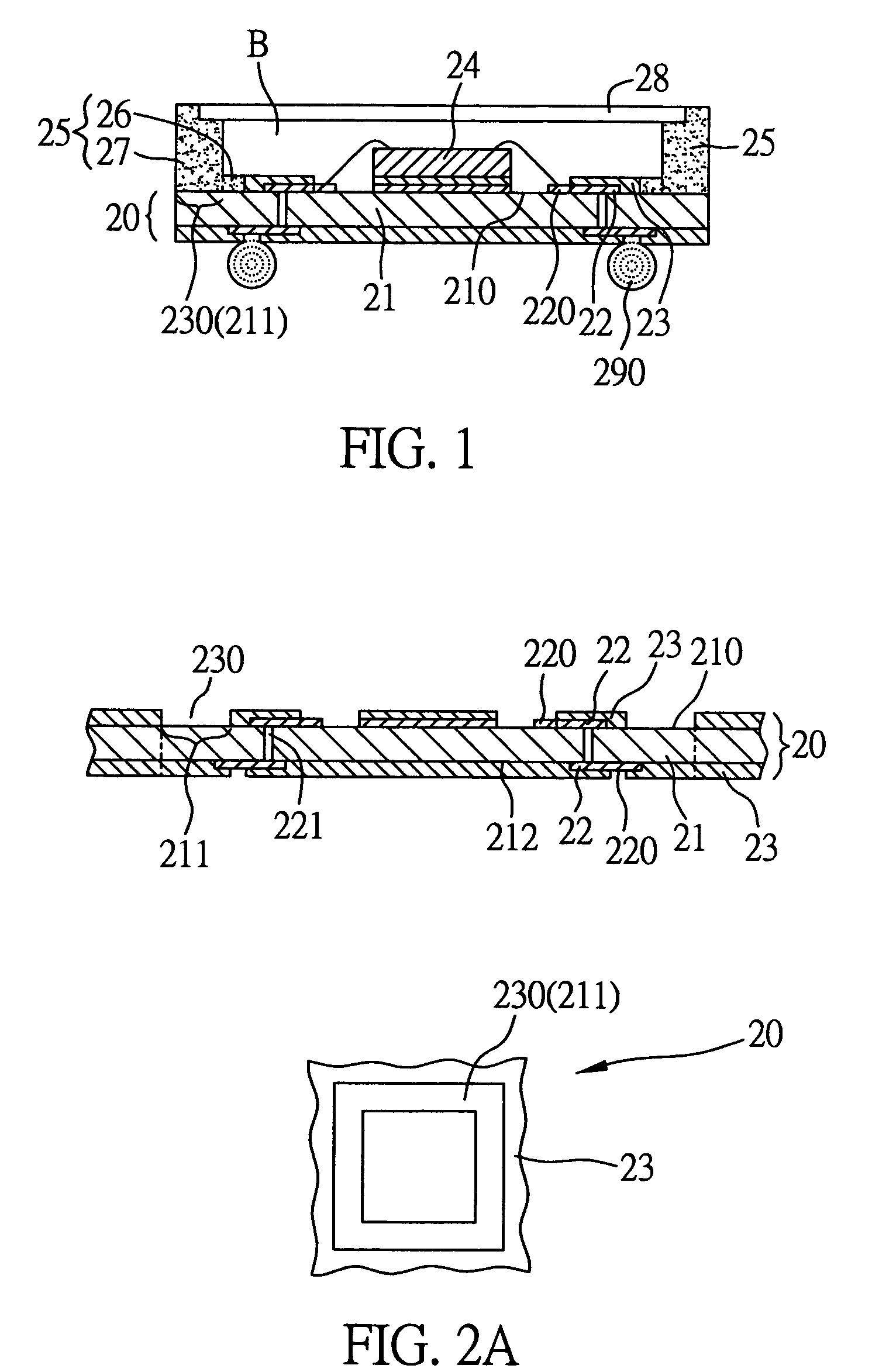
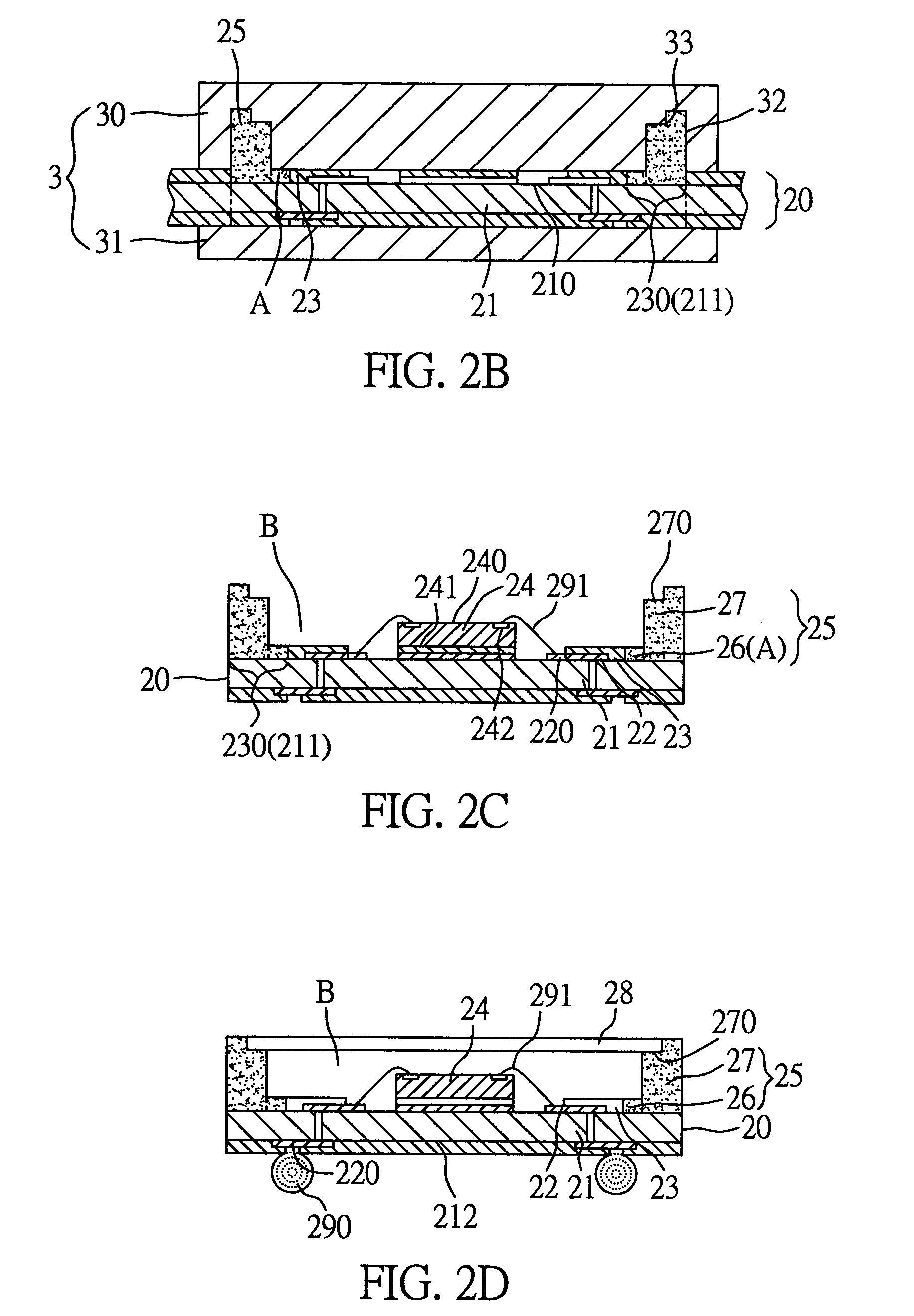
[0017]As shown in FIG. 1, the semiconductor package according to the invention includes a substrate 20 having a core 21 with a plurality of conductive traces 22 formed on at least one surface 210 of the core 21, each conductive trace 22 having a terminal 220, wherein a solder mask layer 23 is applied over the surface 210 of the core 21 and covers the conductive traces 22, allowing the terminals 220 to be exposed to outside of the solder mask layer 23, and the solder mask layer 23 is formed with an opening 230 to expose a continuous peripheral portion 211 on the surface 210 of the core 21; at least one photosensitive chip 24 mounted on the substrate 20 and electrically connected to the exposed terminals 220 of the conductive traces 22; an encapsulation dam 25 formed on the cont...


PUM


Abstract

A semiconductor package with a photosensitive chip and a fabrication method thereof are provided. A substrate having a core is prepared. A solder mask layer is applied over a surface of the core and formed with an opening to expose a continuous peripheral portion on the surface of the core. At least one photosensitive chip is mounted on and electrically connected to the substrate. An encapsulation dam is formed on the continuous peripheral portion of the core and surrounds the chip. The dam includes a shoulder portion adjacent to and flush with the solder mask layer, and a protruded support portion surrounding the shoulder portion. A lid is attached to the support portion of the dam for sealing the dam such that the chip is received in a space defined by the substrate, the dam and the lid.

Description

FIELD OF THE INVENTION[0001]The present invention relates to semiconductor packages and fabrication methods thereof, and more particularly, to a semiconductor package incorporated with at least one photosensitive chip such as CMOS (complementary metal oxide semiconductor) chip, and a method for fabricating the semiconductor package.BACKGROUND OF THE INVENTION[0002]Semiconductor packages are electronic devices for accommodating active components such as semiconductor chips, whose structure is primarily composed of a chip mounted on a substrate and electrically connected to the substrate via conductive elements such as bonding wires; an encapsulation body is formed by a resin compound (such as epoxy resin, etc.) on the substrate to encapsulate the chip and bonding wires which are protected against external moisture and contaminant. The encapsulation body is usually opaque or non-transparent, thereby making a photosensitive chip such as CMOS (complementary metal oxide semiconductor) ch...

Claims


Application Information

Patent Timeline
Patent Type & Authority Patents(United States)
IPC IPC(8): H01L21/00H01L21/44H01L27/146H01L31/0203
CPCH01L27/14618H01L31/0203H01L2224/32225H01L2224/48091H01L2224/48227H01L2224/45144H01L2924/15311H01L2224/73265H01L2224/04042H01L2924/00014H01L2924/00
Inventor HUANG, CHIEN-PINGHSIAO, CHENG-HSUHUANG, CHIH-MING
Owner SILICONWARE PRECISION IND CO LTD
Why Eureka
Try Eureka