Semiconductor memory device and method for programming and erasing a memory cell

a memory cell and memory technology, applied in the field of memory cell programming and erasing methods, can solve the problems of difficult programming of memory cells, threshold voltage exceeding tolerance, and difficulty in containing the threshold voltage range after, so as to shorten the time required for programming processing

Active Publication Date: 2006-02-28
XENOGENIC DEV LLC
View PDF10 Cites 72 Cited by
  • Summary
  • Abstract
  • Description
  • Claims
  • Application Information

AI Technical Summary

Benefits of technology

[0016]It is an object of the present invention to provide a multilevel semiconductor memory device and a multilevel programming method of

Problems solved by technology

However, in the case of the conventional method in which the programming potential and programming time are fixed, and all the memory cells are programmed with data under the same condition, it is difficult to contain the threshold voltage range after the programming of “1” in a tolerance.
Therefore, if the programming characteristics are considered, there are memory cells which can easily be programmed and memory cells which are difficult to be programmed.
With this method, however, the memory cell which is easily programmed is programmed more than necessary, and the threshold voltage exceeds the tolerance.
On the other hand, if threshold voltage of a memory cell programmed with “0” or of a NAND cell from which data is erased becomes greater by certain value in the negative direction, this is also a problem.
However, while the program pulse is applie

Method used


Image

  • Semiconductor memory device and method for programming and erasing a memory cell
  • Semiconductor memory device and method for programming and erasing a memory cell
  • Semiconductor memory device and method for programming and erasing a memory cell

Examples


fourth embodiment

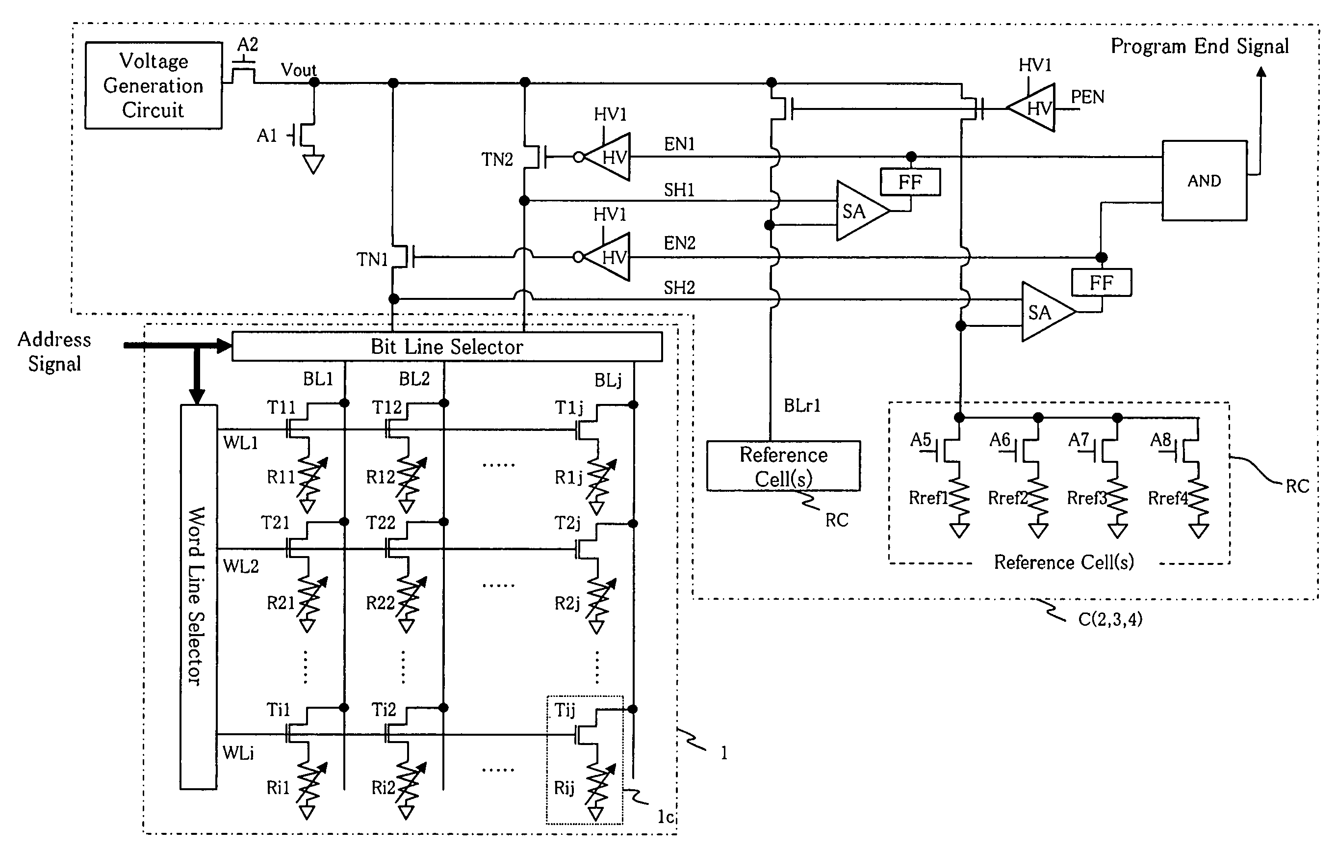
[0063]Next, a fourth embodiment will be explained. FIG. 8 shows one example of a circuit structure having both programming circuit and erasing circuit. Here, a programming circuit All located closer to the bit line selector is added in addition to tan erasing circuit Al0(C′) as a control circuit located closer to the source line selector shown in FIG. 7.

[0064]At the time of programming operation, the program enable signal PEN is brought into high level and the erasing enable signal ERSEN is brought into low level, voltage is supplied to the bit line side, the source line side becomes the ground level and the programming operation is carried out. At that time, control is made such that column switches TN3 and TN4 on the side of the source line become ON state. At the time of erasing operation, the program enable signal PEN is brought into low level, the erasing enable signal ERSEN is brought into high level, voltage is supplied to the source line side, the bit line side becomes the g...

fifth embodiment

[0065]However, in the example shown in FIG. 8, the programming circuit and the erasing circuit require the voltage generating circuit and the sense amplifier, respectively, but if one element can function as both the voltage generating circuit and the sense amplifier, the area can be reduced. This example is shown in FIG. 9 as a This embodiment selects whether the output Vout of the voltage generating circuit should be supplied to the bit line side or source line side by switching the N type MOSFET, and the programming and erasing operations are carried out.

[0066]At the time of programming operation, the program enable signal PEN is brought into high level, and the erasing enable signal ERSEN is brought into low level, the output Vout is supplied to the voltage generating circuit on the bit line side, the source side becomes the ground level and the programming operation is carried out. At the time of erasing operation, the program enable signal PEN is brought into low level, the e...


PUM


Abstract

A semiconductor memory device comprises a memory array in which memory cells having variable resistive elements (R11 to Rij) whose electrical resistance is varied by electrical stress and is held even after the electrical stress is released and selection transistors (T11 to Tij) comprising N type MOSFETs are arranged with a matrix; programming means for applying the electrical stress to the variable resistive elements (R11 to Rij) to program data into the memory cell; programming state detection means for detecting the variation in the electrical resistance at the time of the programming operation; and programming control means for stopping the application of the electrical stress when the electrical resistance is varied to a predetermined reference value. With this structure, it is possible to constitute the semiconductor memory device in which the time required for programming data is shortened and the programming precision is high.

Description

BACKGROUND OF THE INVENON[0001]1. Field of the Invention[0002]The present invention relates to a semiconductor memory device and a programming and erasing method of a memory cell, and more particularly, to a programming and erasing method which can effectively used for a nonvolatile semiconductor memory device using a variable resistive element.[0003]2. Description of the Related Art[0004]As an EEPROM which is a conventional electrically erasable and programmable read-only memory, a NAND cell type EEPROM which can increase the packing density is known. Japanese Unexamined Patent Publication No.H5-182474 describes as follows. In the NAND cell type EEPROM, a plurality of memory cells are connected to each other in series and connected to a bit line as one unit such that the plurality of memory cells use sources and drains of the adjacent memory cells. The memory cell is usually of an FETMOS structure in which a charge-storage layer and a control gate are laminated on each other. A mem...

Claims


Application Information

Patent Timeline
IPC IPC(8): G11C11/00H01L27/108G11C11/56G11C13/00G11C16/34
CPCG11C11/5678G11C11/5685G11C13/0004G11C13/0007G11C13/0038G11C13/004G11C13/0069G11C13/0097G11C13/0064G11C2213/79G11C2013/0054G11C2211/5624G11C2213/31G11C2013/0066H10B12/00
Inventor MATSUOKA, NOBUAKI
Owner XENOGENIC DEV LLC
Why Eureka
Try Eureka