Semiconductor storage device
- Summary
- Abstract
- Description
- Claims
- Application Information
AI Technical Summary
Benefits of technology
Problems solved by technology
Method used
Image
Examples
first embodiment
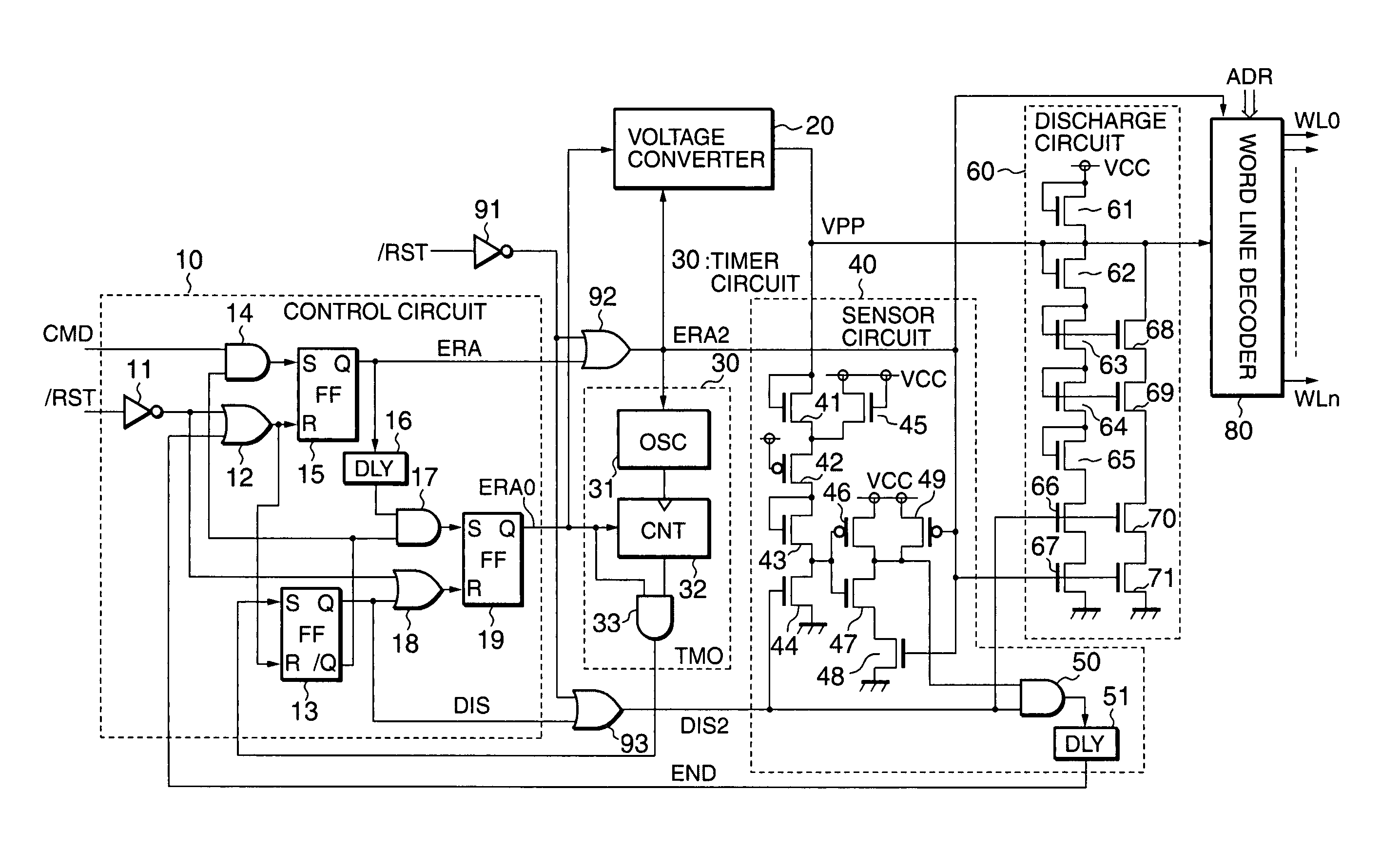
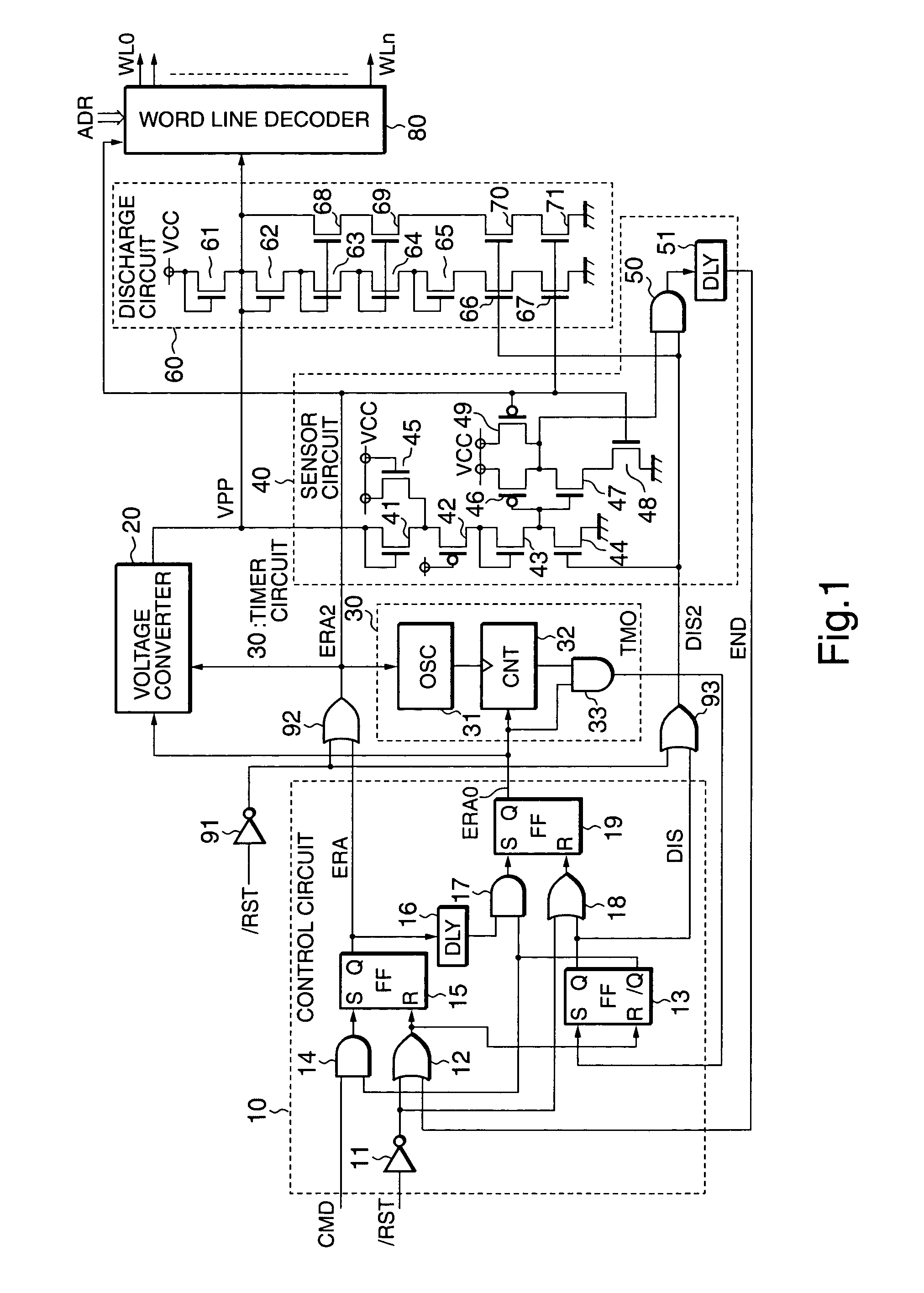
[0022]FIG. 1 is a block diagram showing an erase circuit in a flash memory according to a first embodiment of the present invention.
[0023]The erase circuit comprises a control circuit 10, a voltage converter (booster) 30, a timer circuit 30, a sensor circuit 40, a discharge circuit 60, and a word line decoder 80 for performing erase operations on a memory cell array (not shown in Figs. as a box, but word lines represent the memory cell array). In addition, the erase circuit comprises an inverter 91 and 2-input ORs (OR gates) 92 and 93 to act against a reset condition during erase operations.
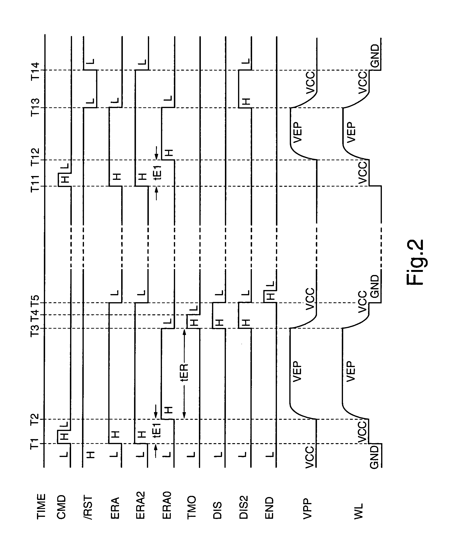
[0024]When supplied with an erase command CMD, the control circuit 10 sequentially outputs an erase start signal ERA and an erase execution signal ERA0 at a specified time interval. When supplied with an erase termination signal TMO, the control circuit 10 stops the erase execution signal ERA0 and outputs a discharge control signal DIS. When supplied with a discharge termination signal END, the c...
second embodiment
[0053]FIG. 3 is a block diagram showing an erase circuit in a flash memory according to a second embodiment of the present invention. The mutually corresponding components in FIGS. 3 and 1 are designated by the same reference numerals and symbols.
[0054]This erase circuit is provided with a pulse circuit 94 in place of the inverter 91 in FIG. 1. The pulse circuit 94 comprises a monostable multivibrator, for example. When the reset signal / RST changes from “H” to “L”, the pulse circuit 94 outputs a pulse signal PLS that goes “H” for a specified period of time tDPL. Accordingly, the OR 92 outputs the erase start signal ERA2 when the erase start signal ERA or the pulse signal PLS is supplied. The OR 93 outputs the discharge control signal DIS2 when the discharge control signal DIS or the pulse signal PLS is supplied. The other configurations are the same as those in FIG. 1.
[0055]FIG. 4 is a signal waveform diagram showing a reset operation during the erase operation in FIG. 3. With refe...
third embodiment
[0064]FIG. 5 is a block diagram showing an erase circuit in a flash memory according to a third embodiment of the present invention. The mutually corresponding components in FIGS. 5 and 1 are designated by the same reference numerals and symbols.
[0065]This erase circuit is provided with a control circuit 10A, an inverter 95, and an OR 96 having configurations slightly different from those of the control circuit 10, the inverter 91, and ORs 92 and 93 of the erase circuit in FIG. 1.
[0066]When supplied with the erase command CMD, the control circuit 10A and the like sequentially output the erase start signal ERA and the erase execution signal ERA0 at a specified time interval. When supplied with the erase termination signal TMO or the reset signal / RST, the control circuit 10A and the like stop the erase execution signal ERA0 and output the discharge control signal DIS. When supplied with the discharge termination signal END, the control circuit 10A and the like stop the erase start si...
PUM
 Abstract
Description
Claims
Application Information
 - R&D Engineer
- R&D Manager
- IP Professional
- Industry Leading Data Capabilities
- Powerful AI technology
- Patent DNA Extraction
Browse by: Latest US Patents, China's latest patents, Technical Efficacy Thesaurus, Application Domain, Technology Topic, Popular Technical Reports.
© 2024 PatSnap. All rights reserved.Legal|Privacy policy|Modern Slavery Act Transparency Statement|Sitemap|About US| Contact US: help@patsnap.com


