Wafer supported, out-of-plane ion trap devices

a technology of ion traps and ion traps, which is applied in the direction of mass spectrometers, separation processes, stability-of-path spectrometers, etc., can solve the problems of large and bulky equipment in which the ion traps are incorporated, complex machining techniques, and high manufacturing costs

Active Publication Date: 2006-03-14
LUCENT TECH INC
View PDF8 Cites 41 Cited by
  • Summary
  • Abstract
  • Description
  • Claims
  • Application Information

AI Technical Summary

Problems solved by technology

Unfortunately, such machining techniques are often complex and costly due to the need for the hyperbolic-shaped inner surfaces 15–17.
Nevertheless, the metallic components of such ion traps are expensive to manufacture and assemble.
Moreover, these metallic components cause equipment in which they are incorporated to be large and bulky.
The latter property has limited the widespread application and deployment of these ion traps in equipment such as mass spectrometers and shift registers.

Method used


Image

  • Wafer supported, out-of-plane ion trap devices
  • Wafer supported, out-of-plane ion trap devices
  • Wafer supported, out-of-plane ion trap devices

Examples


Embodiment Construction

Ion Trap Structure and Operation

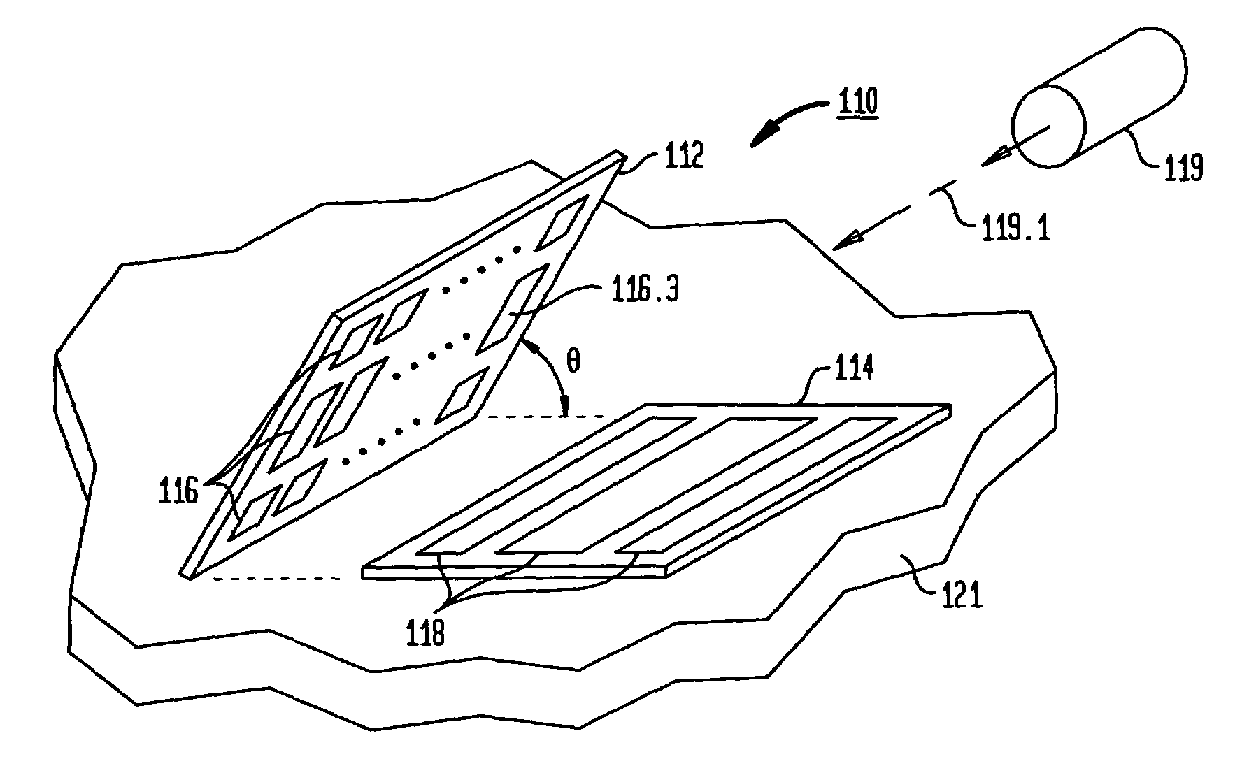
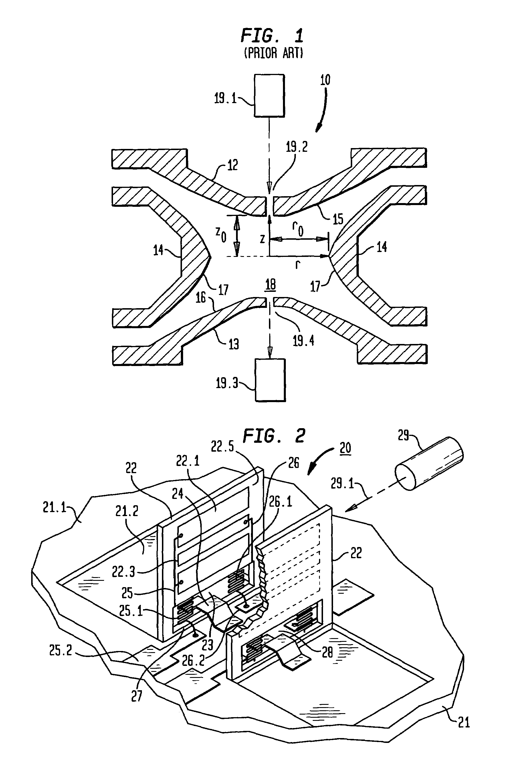
[0027]With reference now to the illustrative embodiment of our invention shown in FIG. 2, a micro-miniature ion trap 20 comprises at least one plate 22, which is rotateably or pivotally mounted on a major surface 21.1 of a wafer (or substrate) 21 during assembly but fixedly mounted on surface 21.1 during operation of the trap. (A pair of plates 22 is shown for purposes of illustration only.) The wafer may be made of semiconductor material, dielectric material, or a combination of both. The ability to pivot or rotate each plate results from processing techniques, which are adapted from the integrated circuit industry and will be described more fully hereinafter. Suffice it to say here that, in one embodiment, such processing results in each plate having a window or aperture 28 formed near the bottom of the electrode so as to define an elongated rail or axle 27, which extends under a hinge 24. When the plate 22 is released from its original as-fabricate...


PUM


Abstract

An ion trap device comprises a wafer that supports at least one plate forming an ion trapping region therebetween. The plate has an electrically insulating surface and a multiplicity of electrodes disposed on the insulating surface. The electrodes form at least one ion trap in the trapping region when suitable voltages are applied to the electrodes via conductors coupled to the wafer. The device has a multiplicity of ports for introducing ions into the trapping region and for extracting ions from that region. In embodiments that include a multiplicity of such plates, a first one of the plates is oriented at a non-zero angle to the major surface of the wafer and is rotateably mounted on that surface. In one embodiment, at least two of the plates form an elongated micro-channel having an axis of ion propagation, and the electrodes on at least one of the two plates are segmented along the direction of the axis, thereby forming a multiplicity of ion traps along the axis. A controller applies suitable voltage (e.g., sequentially) to the segmented electrodes, thereby shifting ions from one trap to another. Preferably, the electrodes on the two plates are segmented. Applications to mass spectrometers and shift registers are described.

Description

BACKGROUND OF THE INVENTION[0001]1. Field of the Invention[0002]This invention relates to ion trap devices and, more particularly, to such devices that are formed by out-of-plane assembly of micro-cavities on a semiconductor or dielectric wafer.[0003]2. Discussion of the Related Art[0004]Conventional ion traps enable ionized particles to be stored and the stored ionized particles to be separated according to the ratio (M / Q) of their mass (M) to their charge (O). Storing the ionized particles involves applying a time-varying voltage to the ion trap so that particles propagate along stable trajectories therein. Separating the ionized particles typically involves applying an additional time-varying voltage to the trap so that the stored particles are selectively ejected according to their M / Q ratios. The ability to eject particles according to their M / Q ratios enables the use of ion traps as mass spectrometers.[0005]Exemplary ion traps are described, for example, by W. Paul et al. in U...

Claims


Application Information

Patent Timeline
Patent Type & Authority Patents(United States)
IPC IPC(8): B01D59/44H01J49/00H01J49/26H01J49/42
CPCH01J49/424H01J49/0018
Inventor AKSYUK, VLADIMIR ANATOLYEVICHPAU, STANLEY
Owner LUCENT TECH INC
Why Eureka
Try Eureka