One chip, low light level color camera

a color camera and low light level technology, applied in the field of low light level imaging devices, can solve the problems of monochromatic image, limited image resolution available at the phosphorous screen, and inability to provide chrominance information in combination with high sensitivity at low light levels, so as to reduce the aliasing of color features

Inactive Publication Date: 2006-03-14
BALL AEROSPACE & TECHNOLOGIES
View PDF30 Cites 59 Cited by
  • Summary
  • Abstract
  • Description
  • Claims
  • Application Information

AI Technical Summary

Problems solved by technology

Although such approaches have had success in providing human perceptible images of scenes that could not otherwise be viewed by the human eye, such approaches have been unable to provide chrominance information in combination with high sensitivity at low light levels.
However, the use of a phosphorous screen results in a monochromatic image.
In addition, the limited resolution of the microchannel element in turn limits the image resolution available at the phosphorous screen.
Furthermore, image intensifiers require a relatively high voltage for operation, and have a finite life span.
However, systems utilizing imagers that are sensitive to infrared wavelengths do not provide information regarding the colors of objects present in the imaged scene.
However, multichip designs are difficult to manufacture and implement.
In addition, the ability of such designs to provide high sensitivity is compromised, by splitting the light gathered by the device's lens system among four different imagers.
Furthermore, the use of four separate image sensors results in an overall package that is relatively large and expensive to produce.
As a result, existing imaging devices that provide color information are relatively insensitive in low light conditions, while imaging devices optimized for high sensitivity and low light conditions typically provide a monochromatic image.
However, because filtering light requires the rejection of at least some components of the light incident on the filter, filtering reduces the sensitivity that might otherwise be available from an imaging device.

Method used


Image

  • One chip, low light level color camera
  • One chip, low light level color camera
  • One chip, low light level color camera

Examples


Embodiment Construction

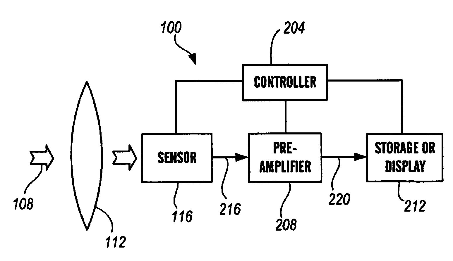
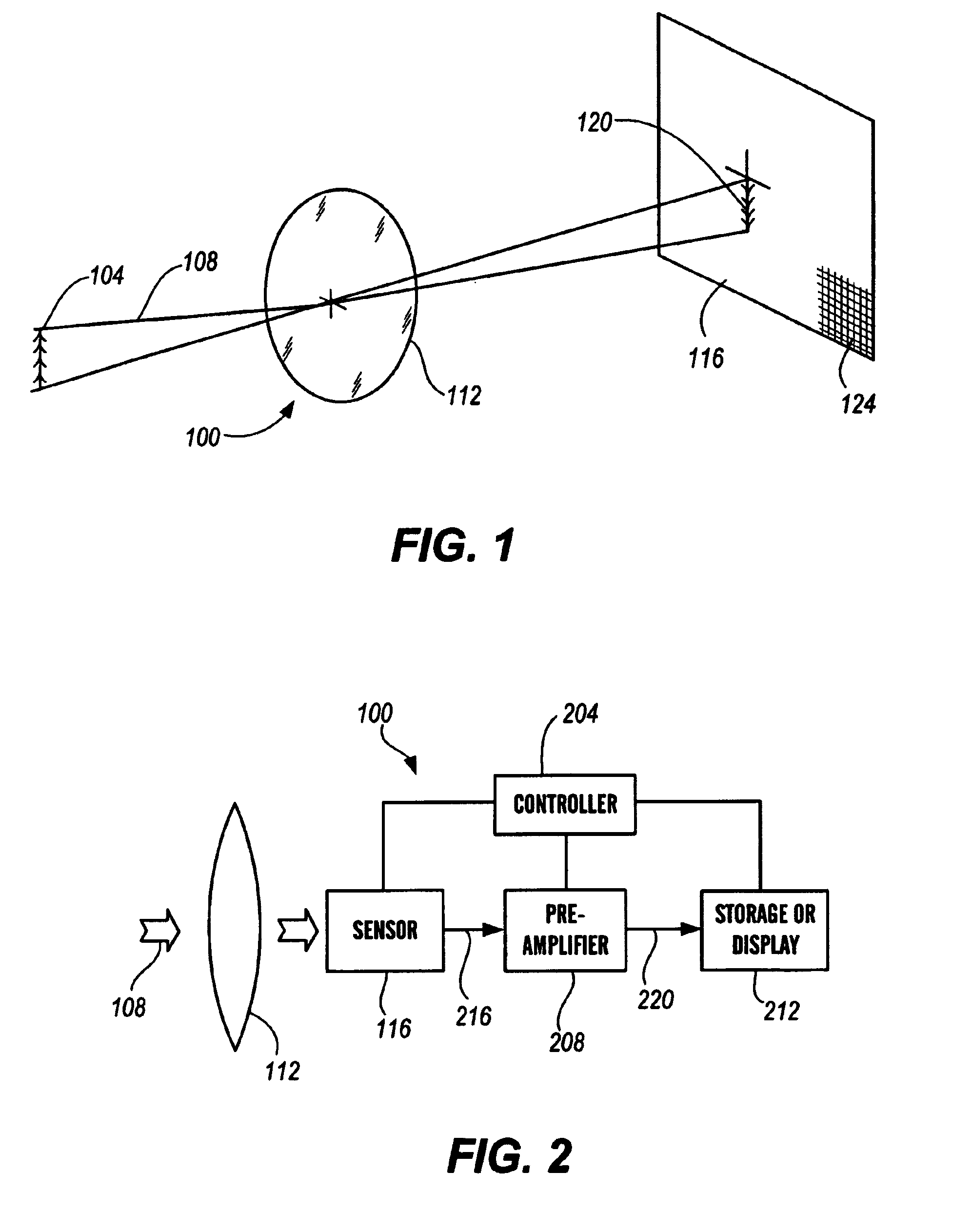
[0037]According to the present invention, a one chip, low light level color imaging device or camera is provided.

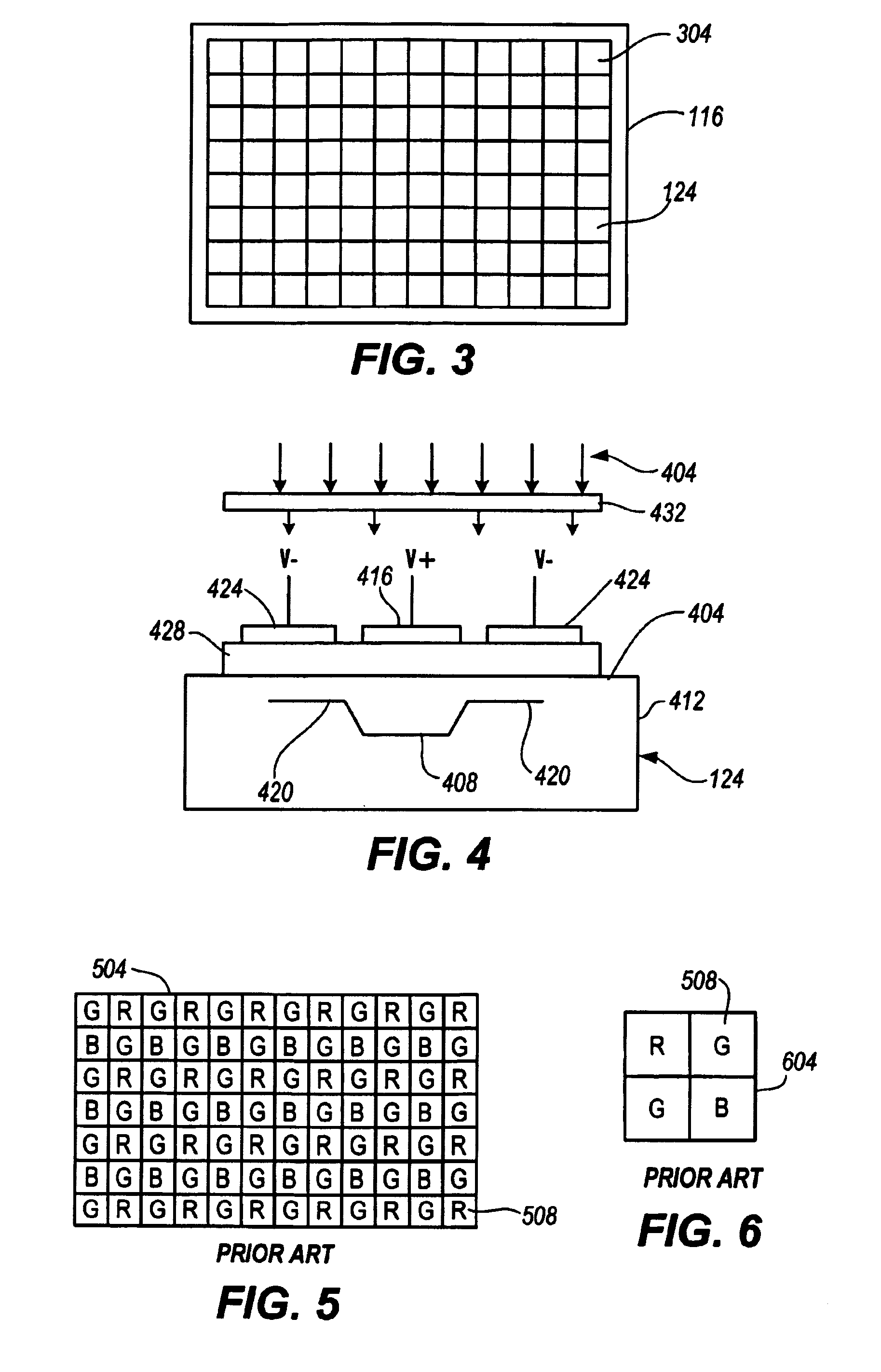
[0038]In FIG. 1, a digital imaging device 100 configuration suitable for use in connection with the present invention is illustrated. As shown in FIG. 1, an object 104 reflects light 108 that is focused by a lens or lens system 112 onto an image sensor 116 as an image object 120. The image sensor 116 is comprised of a plurality of photosensitive elements or pixels 124. The pixels 124 are distributed over the surface of the image sensor 116 in a two-dimensional array. The pixels 124 generally convert the light focused onto the surface of the image sensor 116 by the lens 112 (i.e. the image object 120) into electronic signals.

[0039]In a conventional color imaging device, each of the pixels 124 of the image sensor 116 receive light within one of three overlapping frequency bands. The relative intensity of the light received by individual pixels 124 included in a group of pix...


PUM


Abstract

A high sensitivity, single chip, low light level imaging device is provided. The imaging device of the present invention utilizes sparse color sampling, to maximize the luminance information gathered. In particular, color information is gathered by a small proportion of the pixels included in an image sensor, while the remaining pixels operate at full spectrum sensitivity. The present invention allows the correct hue of objects to be determined, while providing high sensitivity to available luminance information in a scene. In addition, the present invention allows hue information to be ascribed to objects in a scene, even in combination with luminance data collected over a spectrum that includes the near infrared and infrared wavelengths.

Description

FIELD OF THE INVENTION[0001]The present invention relates to low light level imaging devices. In particular, the present invention relates to electronic low light level imaging devices that are sensitive to infrared wavelengths and that are capable of providing color information.BACKGROUND OF THE INVENTION[0002]Low light level imaging devices are useful in a wide variety of applications. For example, low light level imaging devices are useful in nighttime surveillance activities. In low light level conditions, it is important for sensors to take advantage of every available photon. Approaches to providing human perceptible images in low light conditions have included the use of image intensifiers. Other approaches to providing images in low light conditions have utilized the detection of light having wavelengths outside of the visible spectrum. Although such approaches have had success in providing human perceptible images of scenes that could not otherwise be viewed by the human ey...

Claims


Application Information

Patent Timeline
Patent Type & Authority Patents(United States)
IPC IPC(8): H04N3/14H04N5/335H04N9/04H04N9/083H01L27/148H04N5/225H04N9/07
CPCH04N5/332H04N9/045H04N2209/047H04N2209/045H04N23/11H04N23/843H04N25/134
Inventor FRAME, WAYNE W.
Owner BALL AEROSPACE & TECHNOLOGIES
Why Eureka
Try Eureka