Method of growing single crystal Gallium Nitride on silicon substrate

a gallium nitride and silicon substrate technology, applied in the direction of crystal growth process, polycrystalline material growth, chemically reactive gas, etc., can solve the problems of difficult to achieve high-quality gan buffer layer, inconvenient commercialization, and inability to meet the needs of the mark

Inactive Publication Date: 2006-03-21
NAT CHENG KUNG UNIV
View PDF1 Cites 22 Cited by
  • Summary
  • Abstract
  • Description
  • Claims
  • Application Information

AI Technical Summary

Benefits of technology

[0005]An object of the present invention is to provide a method of growing Silicon Carbon Nitride(SiCN) film as buffer layer to help grow GaN elements, and to break trough bottleneck of hetero-structure eptiaxy technology. Another object of the present invention is to utilize SiCN buffer layer which eliminates lattice mismatch between GaN and silicon wafer to substitute sapphire and SiC substrates for security of GaN elements quality and obvious discount of manufacturing cost.

Problems solved by technology

At the present, GaN grows on sapphire or silicon carbide substrates, however those two substrates are expensive, and it is not easy to integrate with silicon s miconductor which is mature and cheap, and consequently the market growth of those two technology is retarded.
Owing to 16% lattice mismatch between sapphire and GaN, it is difficult to achieve high quality GaN buffer layer.
Silicon carbide is another potential substrate material, because of its only 3% lattice mismatch between SiC and GaN, good electric and thermal conductivity, but it is very expensive, and not suitable to commercialize.
However, grow directly GaN on silicon wafer will results in high density of defects and cracks, and consequently the hetero-structure eptiaxy technology is retarded.

Method used


Image

  • Method of growing single crystal Gallium Nitride on silicon substrate
  • Method of growing single crystal Gallium Nitride on silicon substrate
  • Method of growing single crystal Gallium Nitride on silicon substrate

Examples


embodiment

PREFERRED EMBODIMENT

[0023]By referring to the following description and accompanying drawings, preferred embodiment will be demonstrated clearly.

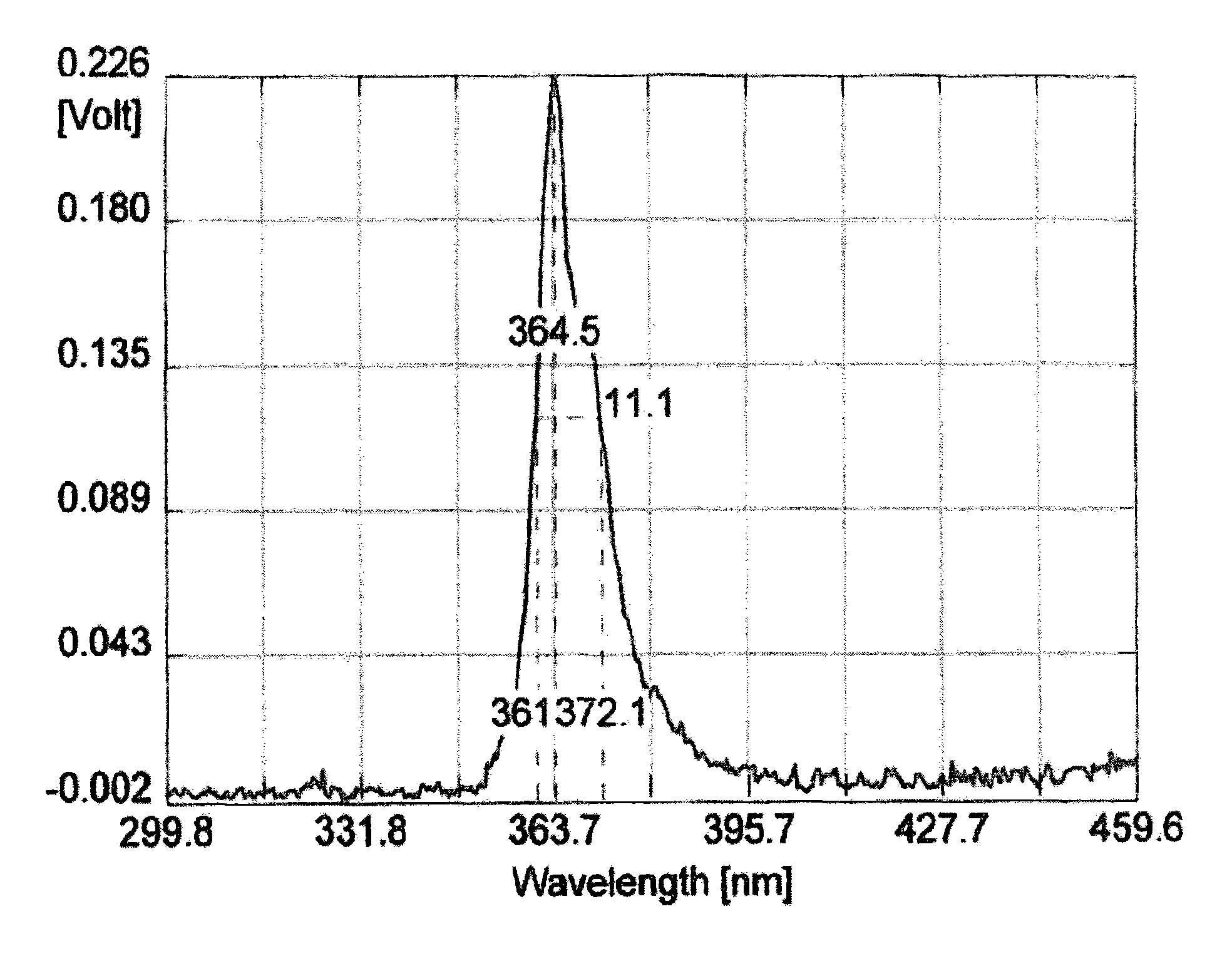
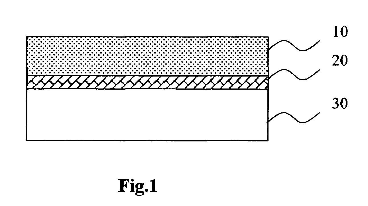
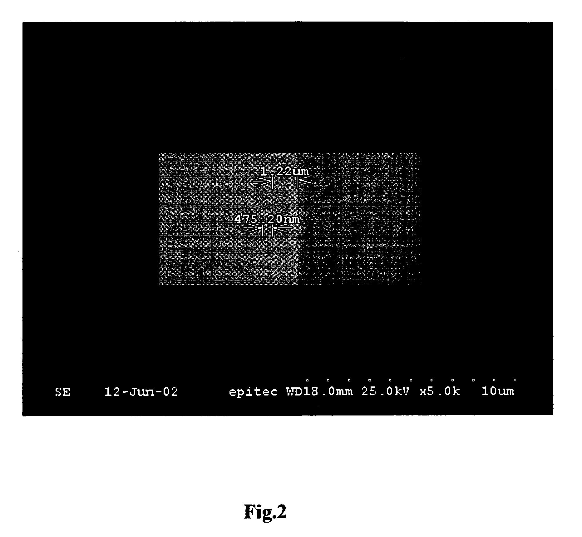
[0024]The preferred embodiment of the present invention adopts n-type silicon crystal chip oriented in direction as substrate 10, 400±25 μm in thickness, with specific resistivity ranging from 4 ohm-cm to 10 ohm-cm. The said embodiment adopts RTCVD system to remove oxide layer on silicon substrate 10 and to grow a SiCN buffer layer 20, about 4750 Å in thickness, which eliminates lattice mismatch between silicon substrate 10 and GaN 30, and then adopts MOCVD system to grow a single crystal GaN thin film 30 on SiCN buffer layer 20, wherein a GaN buffer layer about 200 Å to 300 Å in thickness is grown at lower growing temperature ranging from 500° C. to 600° C., and then the formal single crystal GaN thin film about 1.2 μm in thickness grown at higher growing temperature ranging from 1000° C. to 1100 C. GaN thin film thus fabricated is the ac...


PUM

PropertyMeasurementUnit
pressureaaaaaaaaaa
temperatureaaaaaaaaaa

Abstract

A method of growing single crystal Gallium Nitride on silicon substrate is disclosed including: removing oxide layer of silicon substrate, growing buffer layer of Silicon Carbon Nitride (SiCN), and growing single crystalline Gallium Nitride thin film, characterized in that a buffer layer of SiCN is grown to avoid lattice mismatch which appears when Gallium Nitride is grown directly on silicon substrate, and that Rapid Thermal Chemical Vapor Deposition is adopted to grow SiCN buffer layer, and that Metalorganic Chemical Vapor Deposition is adopted to grow single crystalline GaN thin film. The method of present invention has advantages: a) eliminating lattice mismatch between GaN and Si effectively, b) taking the place of sapphire substrate which has high lattice mismatch, and SiC substrate which is expensive, c) intergrating with maturely-developed, cheap silicon semiconductor industry, d) being compatible with VLSI technology, e) being fabricated in large area substrate, f) no need of isolated etching, g) smaller dimension of each unit GaN element, h) convenience to fabricate vertical-structured LED or LD element, I) promoting GaN elements quality, j) increasing yield, k) reducing manufacturing cost.

Description

BACKGROUND OF THE INVENTION[0001]1. Field of the Invention[0002]The present invention relates to a method of growing single crystal Gallium Nitride (GaN), particularly to a method of growing single crystal Gallium Nitride (GaN) on silicon substrate.[0003]2. Description of Related Art[0004]Due to rapid advance of researching and fabrication of ultraviolet to blue optoelectronic elements, such as blue light emitting diode, blue LASER semiconductor, ultraviolet sensor, GaN has been one of the most important wide-band-gap semiconductor materials in group III nitride. At the present, GaN grows on sapphire or silicon carbide substrates, however those two substrates are expensive, and it is not easy to integrate with silicon s miconductor which is mature and cheap, and consequently the market growth of those two technology is retarded. Owing to wide application range, mature and cheap silicon technology, advantage and potential of growing GaN elements on silicon wafer is expected. It is be...

Claims


Application Information

Patent Timeline
Patent Type & Authority Patents(United States)
IPC IPC(8): C30B25/12C30B25/14C23C16/42C30B25/02H01L21/205
CPCC30B25/02C30B29/406C30B29/403
Inventor FANG, YEAN KUENCHANG, WEN RONGTING, SHYH FANNKUAN, HONCHANG, CHENG NAN
Owner NAT CHENG KUNG UNIV
Why Eureka
Try Eureka