
Patterned thin film graphite devices and method for making same

a graphite device and thin film technology, applied in the field of thin film graphite electronic devices, can solve the problems of carbon nanotube-based molecular electronics, the reduction of contact power, and the ultimate limit of silicon-based electronics in the near future, and achieve the effect of greatly reducing or eliminating power dissipation at the contacts

Active Publication Date: 2006-03-21
GEORGIA TECH RES CORP
View PDF5 Cites 124 Cited by
  • Summary
  • Abstract
  • Description
  • Claims
  • Application Information

AI Technical Summary

Benefits of technology

[0016]Integrated electronics based on ultra-thin graphite film (UTGF) have several advantages over prior art, these include: large-scale integration is possible using standard microelectronics lithography methods; metals are not used to interconnect the devices so that metal-to-graphite contact resistances are avoided and power dissipation at the contacts is greatly reduced or eliminated; integrated electronic device structures whose operation relies on quantum interference effects can be constructed; feature sizes as small as 1 nm scale are possible and limited only by the lithography methods; and graphite can be electronically modified by chemically bonding molecules to the edges of graphite strips, without damaging the graphitic structure.

Problems solved by technology

However, miniaturization of silicon-based electronics will reach an ultimate limit in the near future, primarily because of limitations imposed by the material properties of silicon, and doped silicon, at the nanoscale.
However, none of the proposed alternatives fulfills all three of the above-listed requirements.
Despite the advantages mentioned above, there are also important disadvantages associated with carbon nanotube-based molecular electronics.
This aspect by itself currently prohibits large-scale integration of nanotubes.
Because of these disadvantages, nanotubes are not used yet in commercial integrated electronic circuits.
Moreover, integration of carbon nanotube-based electronic devices on a large scale is not expected to be feasible in the foreseeable future.

Method used


Image

  • Patterned thin film graphite devices and method for making same
  • Patterned thin film graphite devices and method for making same
  • Patterned thin film graphite devices and method for making same

Examples


Embodiment Construction

[0025]A preferred embodiment of the invention is now described in detail. Referring to the drawings, like numbers indicate like parts throughout the views. As used in the description herein and throughout the claims, the following terms take the meanings explicitly associated herein, unless the context clearly dictates otherwise: the meaning of “a,”“an,” and “the” includes plural reference, the meaning of “in” includes “in” and “on.”“Annealing” includes processes in which a substance is heated to a temperature that causes a physical change in the substance, and is not limited to the heating and cooling of metals.

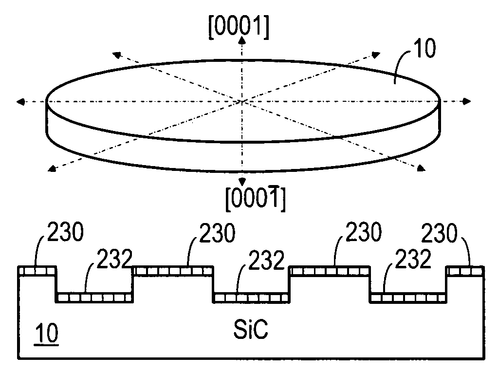
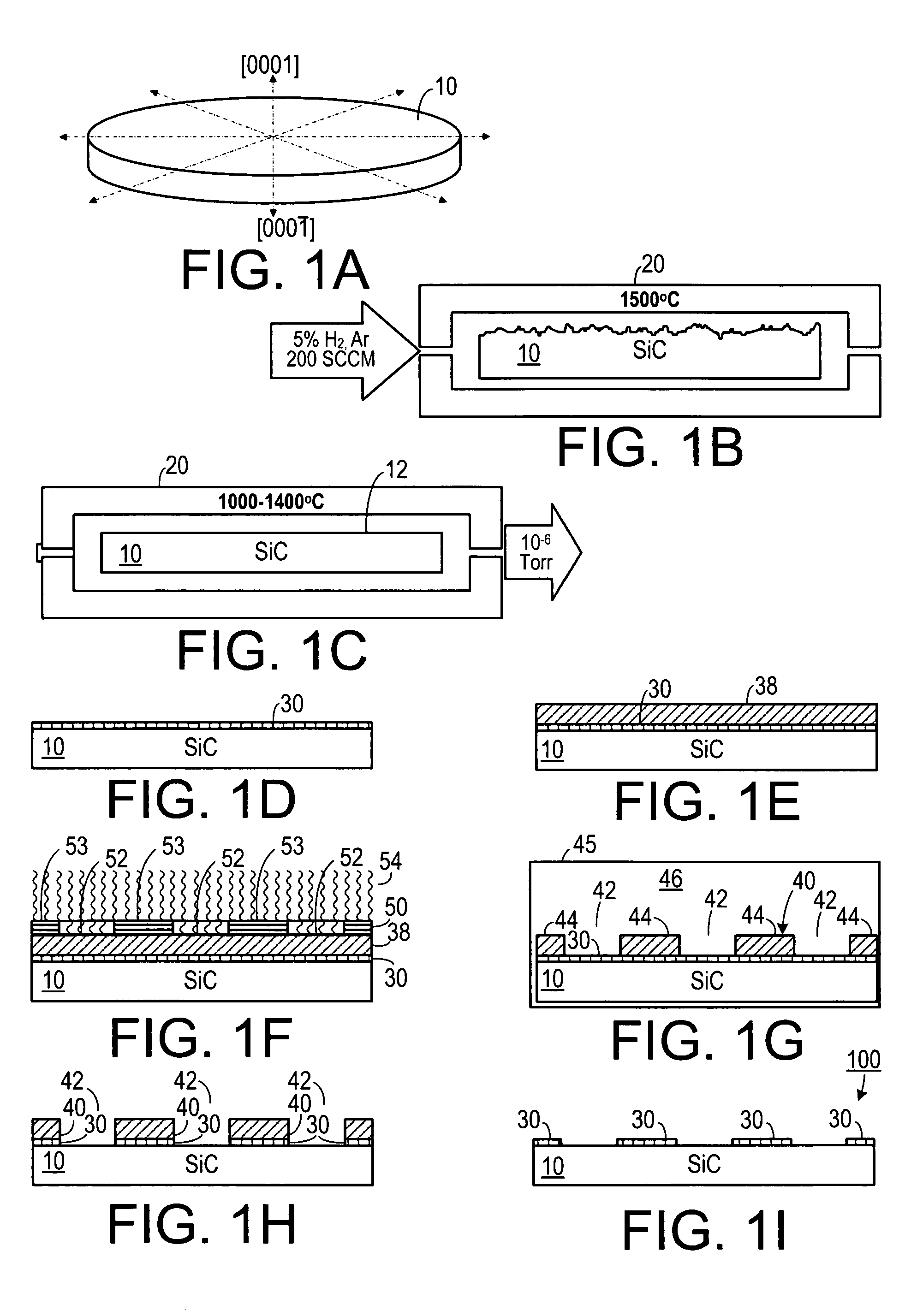
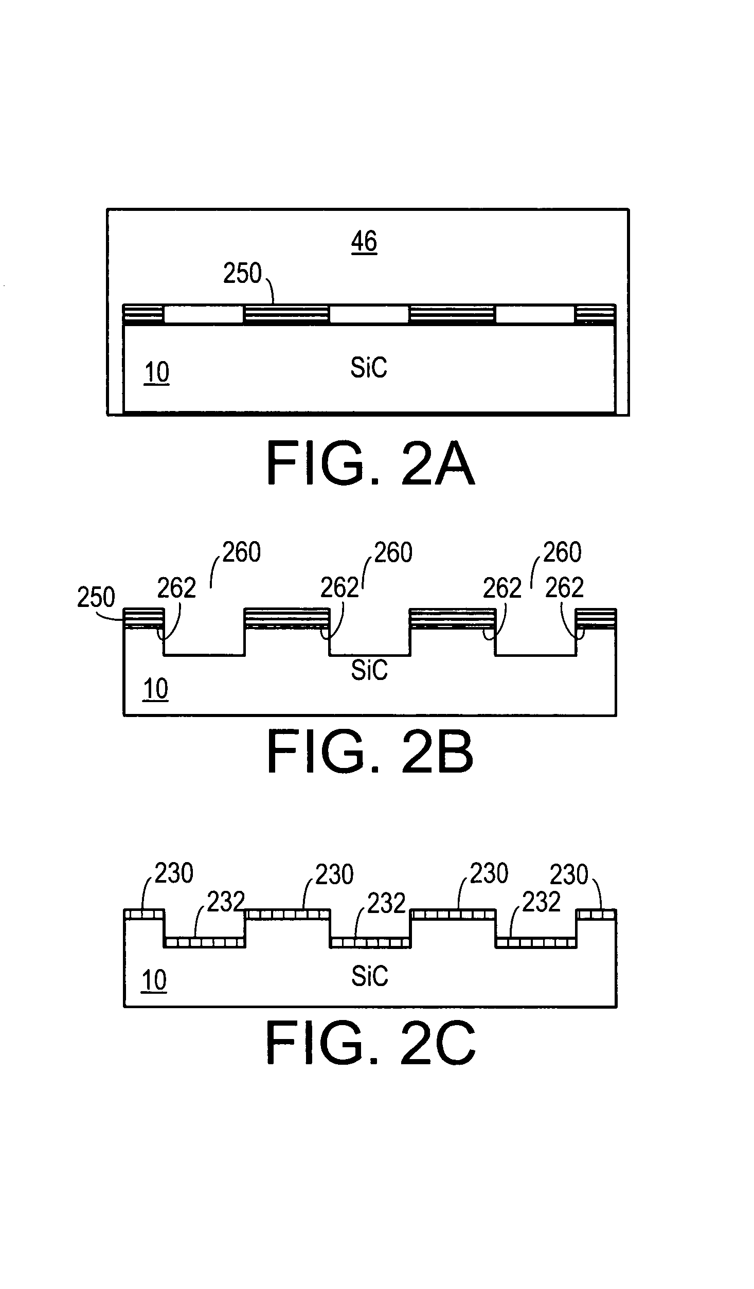
[0026]As shown in FIG. 1A, one method of making a device according to the invention begins with a substrate 10, such as a crystalline substrate. One example of a crystalline substrate includes silicon carbide. In one embodiment, a 6H crystal of silicon carbide was used and a device according to the invention was produced on the [0001] face of the crystal. As will be apprecia...


PUM


Abstract

In a method of making graphite devices, a preselected crystal face of a crystal is annealed to create a thin-film graphitic layer disposed against selected face. A preselected pattern is generated on the thin-film graphitic layer. A functional structure includes a crystalline substrate having a preselected crystal face. A thin-film graphitic layer is disposed on the preselected crystal face. The thin-film graphitic layer is patterned so as to define at least one functional structure.

Description

CROSS-REFERENCE TO A PROVISIONAL PATENT APPLICATION[0001]The present application claims priority on U.S. Provisional Patent Application Ser. No. 60 / 477,997, filed Jun. 12, 2003, entitled “METHOD TO MAKE INTEGRATED AND DISCRETE ELECTRONIC COMPONENTS FROM STRUCTURED THIN GRAPHITIC MATERIALS,” the entirety of which is incorporated herein by reference into the disclosure of the present application.BACKGROUND OF THE INVENTION[0002]1. Field of the Invention[0003]The present invention relates to thin film electronic devices and, more specifically, to a system for making thin film graphitic devices.[0004]2. Description of the Prior Art[0005]In modern microelectronics integrated-circuit technology, a silicon wafer is lithographically patterned to accommodate a large number of interconnected electronic components (field effect transistors, resistors, capacitors, etc). The technology relies on the semiconducting properties of silicon and on lithographic patterning methods. Increasing the densi...

Claims


Application Information

Patent Timeline
IPC IPC(8): H01L21/461B32B9/00H01LH01L21/04H01L21/302H01L29/16H01L29/772
CPCH01L21/0405H01L21/0445H01L29/16H01L29/772H01L29/7781H01L29/1606Y10S438/931
Inventor DEHEER, WALT A.BERGER, CLAIREFIRST, PHILLIP N.
Owner GEORGIA TECH RES CORP
Features
  • Generate Ideas
  • Intellectual Property
  • Life Sciences
  • Materials
  • Tech Scout
  • Unparalleled Data Quality
  • Higher Quality Content
  • 60% Fewer Hallucinations
Learn More