Multi-chips module assembly package

a technology of module and assembly package, which is applied in the direction of printed circuit manufacturing, printed circuit electric connection formation, printed circuit aspects, etc., can solve the problems of landless design process, size limitation, and inability to meet the requirements of landless design, and the integration circuit packaging technology is becoming a limiting factor for the development of packaged integrated circuits of higher performan

Active Publication Date: 2006-03-21
ADVANCED SEMICON ENG INC
View PDF0 Cites 103 Cited by
  • Summary
  • Abstract
  • Description
  • Claims
  • Application Information

AI Technical Summary

Benefits of technology

[0014]As mentioned above, the via of the intermediate substrate has a plurality of separated electrically conductive layers formed therein and said conductive layers are electrically isolated from each other, so the number of the conductive devices electrically connecting to the conductive layers for transmitting the signals to external devices will be increased.

Problems solved by technology

Recently, integrated circuit (chip) packaging technology is becoming a limiting factor for the development in packaged integrated circuits of higher performance.
Semiconductor package designers are struggling to keep pace with the increase in pin count, size limitations, low profile, and other evolving requirements for packaging and mounting integrated circuits.
However, the process of the landless design is complex and the cost is increased.
Consequently, it will be difficult to fabricate this kind of intermediate substrate.
Besides, the quality of the electricity will be seriously affected in that, with reference to FIG. 6, the bent portions of the conductive traces and the distance of the signal transmission are increased.
However, the fabrication method of plating metal layer on the inner wall of the via 240 will become more complex due to the smaller diameter of the via 240.

Method used


Image

  • Multi-chips module assembly package
  • Multi-chips module assembly package
  • Multi-chips module assembly package

Examples


Embodiment Construction

[0030]The multi-chips module assembly package according to the preferred embodiment of this invention will be described herein below with reference to the accompanying drawings, wherein the same reference numbers refer to the same elements.

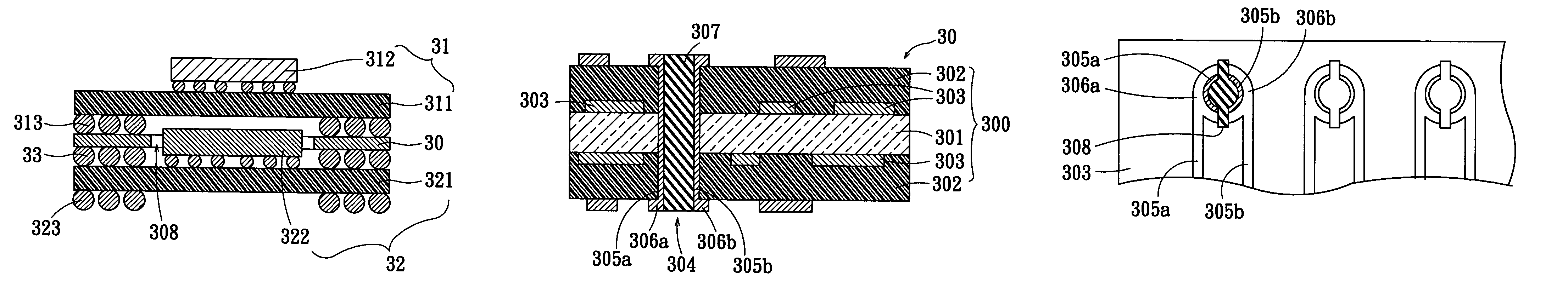
[0031]In accordance with a first preferred embodiment as shown from FIG. 7 to FIG. 10, there is provided a multi-chips module assembly package. The multi-chips module assembly package mainly comprises an intermediate substrate 30, a first package 31 and a second package 32. The first package 31 at least comprises a first substrate 311 and a first chip 312, wherein the first chip 312 is electrically connected to the first substrate 311 by flip-chip bonding. Similarly, The second package 32 at least comprises a second substrate 321 and a second chip 322, wherein the second chip 322 is electrically connected to the second substrate 321 by flip-chip bonding, and disposed in the opening 308 of the intermediate substrate 30. Thus, the second package 32 ...


PUM


Abstract

A multi-chips module assembly package mainly comprises a first package, a second package and an intermediate substrate. The intermediate substrate includes an opening, at least a via and a plurality of circuit layers, wherein the second package is accommodated in the opening. The via has an inner wall, and a plurality of separated electrically conductive layers, which is formed on the inner wall and connected with the corresponding circuit layers. The first package electrically connects with the second package through the intermediate substrate, and the intermediate substrate is interposed between the first package and the second package. At least an insulator is formed in the via, and the separated electrically conductive layers are separated from each other. After the intermediate substrate is interposed between the first package and the second package, there will be not enough space between the intermediate substrate, the first package and the second package for disposing conductive devices therein. Therefore, the first package will be electrically connected to the second package through the separated electrically conductive layers of the intermediate substrate for providing more conductive devices disposed and interposed between the intermediate substrate, the first package and the second package.

Description

BACKGROUND OF THE INVENTION[0001]1. Field of Invention[0002]This invention relates to a multi-chips module assembly package. More particularly, the present invention is related to a multi-chips module assembly package having an intermediate substrate with a via, wherein the via has a plurality of electrically conductive layers formed therein and electrically isolated from each other.[0003]2. Related Art[0004]Recently, integrated circuit (chip) packaging technology is becoming a limiting factor for the development in packaged integrated circuits of higher performance. Semiconductor package designers are struggling to keep pace with the increase in pin count, size limitations, low profile, and other evolving requirements for packaging and mounting integrated circuits.[0005]Due to the assembly package in miniature and the integrated circuits operation in high frequency, MCM (multi-chips module) package is commonly used in said assembly package and electronic devices. Usually, said MCM ...

Claims


Application Information

Patent Timeline
Patent Type & Authority Patents(United States)
IPC IPC(8): H01L23/02H01L23/48H01L23/52H01L29/40H01L25/10H05K1/14H05K3/34H05K3/42
CPCH01L25/105H05K1/144H01L2924/01078H01L2924/15311H05K1/141H05K3/3436H01L2224/16225H05K2201/045H05K2201/0959H05K2201/09645H05K2201/10378H01L2225/1023H01L2225/107H05K3/429
Inventor CHANG, CHIH-HUANGLEE, SHIH-CHANG
Owner ADVANCED SEMICON ENG INC
Why Eureka
Try Eureka