Page buffer for NAND flash memory

a nand flash memory and buffer technology, applied in static storage, digital storage, instruments, etc., can solve the problem of increasing the chip area, and achieve the effect of increasing the data loading speed and reducing the chip area

Inactive Publication Date: 2006-03-21
SK HYNIX INC
View PDF4 Cites 39 Cited by
  • Summary
  • Abstract
  • Description
  • Claims
  • Application Information

AI Technical Summary

Benefits of technology

[0018]The Accordingly, the present invention is directed to provide a page buffer of a

Problems solved by technology

Thus, there is a problem that a chip area becomes lar

Method used


Image

  • Page buffer for NAND flash memory
  • Page buffer for NAND flash memory
  • Page buffer for NAND flash memory

Examples


Embodiment Construction

[0029]Now, embodiments of the present invention will be described in detail with reference to the accompany drawings.

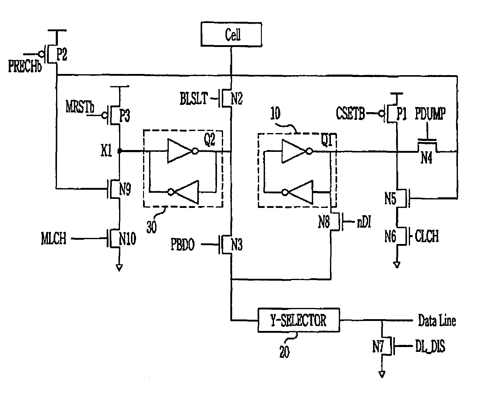
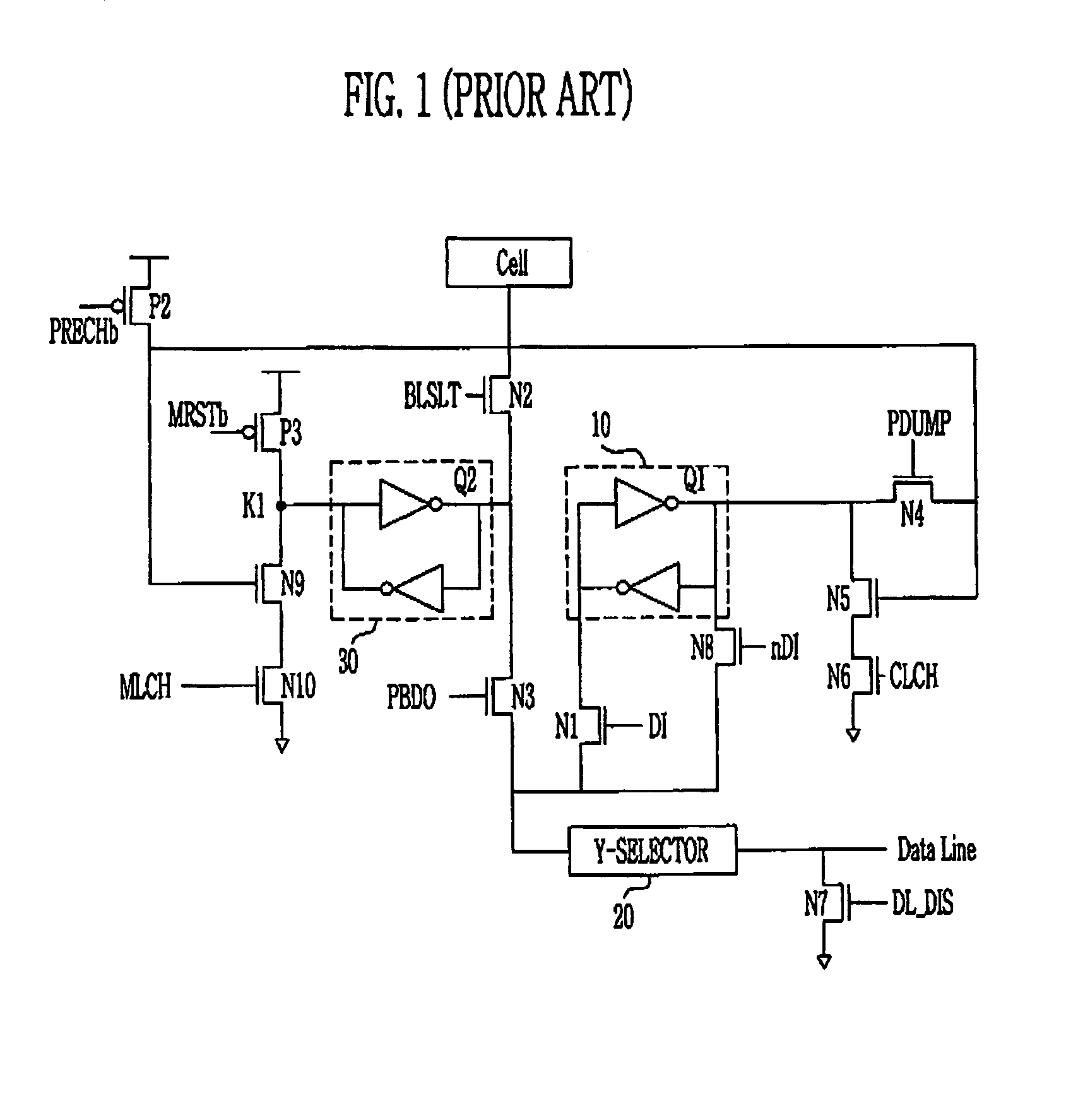
[0030]FIG. 3 is a circuit diagram showing a page buffer of an NAND flash memory according to the present invention. The operation of the NAND flash memory circuit diagram will be described with reference to FIGS. 4A and 4B.

[0031]An NMOS transistor N2 is turned-on depending on a bit line selection signal, so that the data stored on a memory cell is stored on a second latch 30. When a page buffer data output signal PBDO is activated, an NMOS transistor N1 is turned-on, so that the data stored on the second latch 30 are transferred to a data line through a column selector (Y-selector) 20.

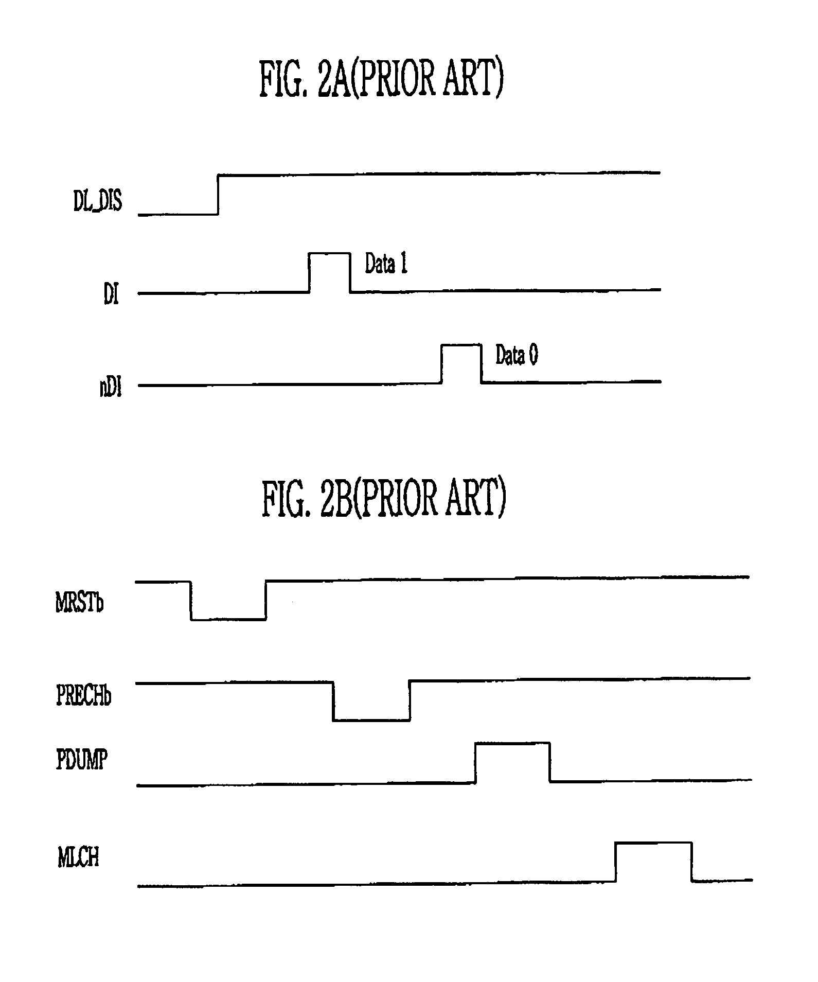
[0032]In order to load data to a latch 10, a cache set bar signal CSETB of FIG. 4A is in a low level, so that a node Q1 of the first latch 10 becomes a high level. When a data line discharge signal DL_DIS is activated in a high level, an NMOS transistor N7 is turned-on, so that charges o...


PUM


Abstract

A page buffer for an NAND flash memory, including: a first latch for loading data; a second latch for storing data stored on a cell depending on a bit line selection signal; a setting circuit for setting the first latch to a high level to load data in a high level; a first switching circuit for transferring the data stored on the second latch depending on a data output signal of a page buffer; a discharging circuit for discharging charges on a data line; a second switching circuit for connecting the data line discharged by the discharging circuit to the first latch depending on a data control signal to load the data in a low level to the first latch; and a data transferring circuit for transferring the data of the first latch to the second latch.

Description

BACKGROUND[0001]1. Field of the Invention[0002]The present invention relates to a page buffer for an NAND flash memory and, more specifically, to a pager buffer for an NAND flash memory capable of improving data loading speed depending on contents of data to be programmed.[0003]2. Discussion of Related Art[0004]Recently, demands for semiconductor memory devices capable of electrically programming, erasing and storing data, even in case that a power source is not supplied, has been increased. Further, in order to develop a large capacity memory device capable of storing an amount of data, a high-integration technology of a memory cell has been developed. As a result, an NAND type of a flash memory device, in which a plurality of memory cells are serially connected to constitute one string and a memory cell array includes a plurality of strings, has been proposed.[0005]A flash memory cell of the NAND flash memory device comprise a current path formed between a source and a drain on a ...

Claims


Application Information

Patent Timeline
IPC IPC(8): G11C16/04G11C16/06G11C7/10G11C16/02G11C16/24
CPCG11C7/1021G11C16/24G11C7/106G11C7/1051G11C16/06
Inventor KIM, DOE COOK
Owner SK HYNIX INC
Why Eureka
Try Eureka