Light emitting device having both electrodes formed on the insulating layer

a technology of insulating layer and light emitting device, which is applied in the direction of discharge tube/lamp details, organic semiconductor devices, discharge tube luminescnet screens, etc., can solve the problems of small work function of cathode and general intransparency of its substan

Inactive Publication Date: 2006-03-28
SEMICON ENERGY LAB CO LTD
View PDF13 Cites 15 Cited by
  • Summary
  • Abstract
  • Description
  • Claims
  • Application Information

AI Technical Summary

Benefits of technology

[0010]In FIG. 12, when an angle formed by the side surface of the electrode and the surface of the substrate is given as “A”, the angle “A” is set to be 30° to 90° (preferably, 50° to 70°). When the angle “A” is made small, a film can be formed such that a change in the thickness of the light emitting layer is less in corner portions of the electrode and portions in which the electrode is in contact with the surface of the substrate.

Problems solved by technology

In addition, generally, a cathode in which a work function is small is not transparent.
In addition, in the light emitting element, although the cathode in which a work function is small is used, its substance is not generally transparent.

Method used


Image

  • Light emitting device having both electrodes formed on the insulating layer
  • Light emitting device having both electrodes formed on the insulating layer
  • Light emitting device having both electrodes formed on the insulating layer

Examples


embodiment 1

[Embodiment 1]

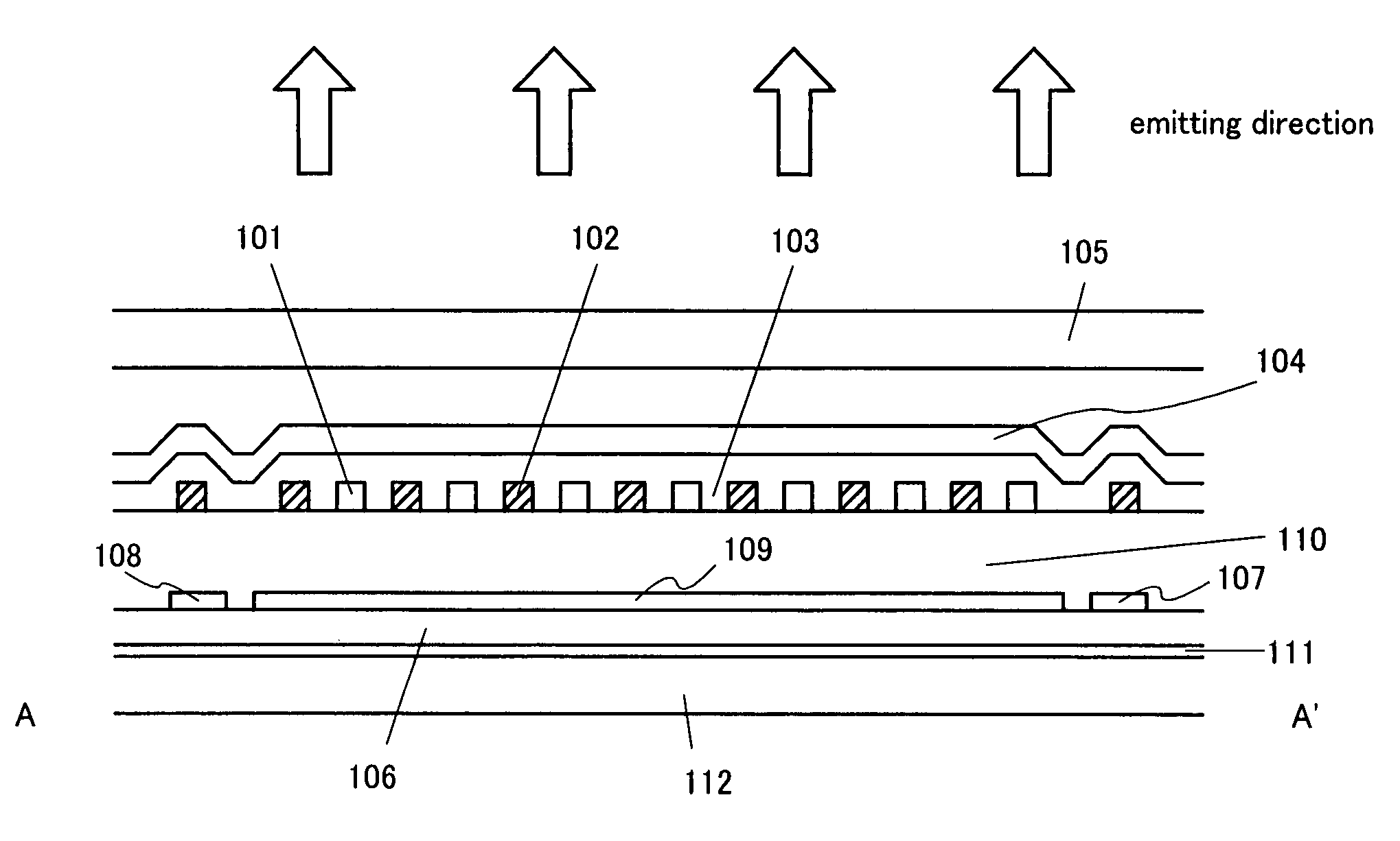
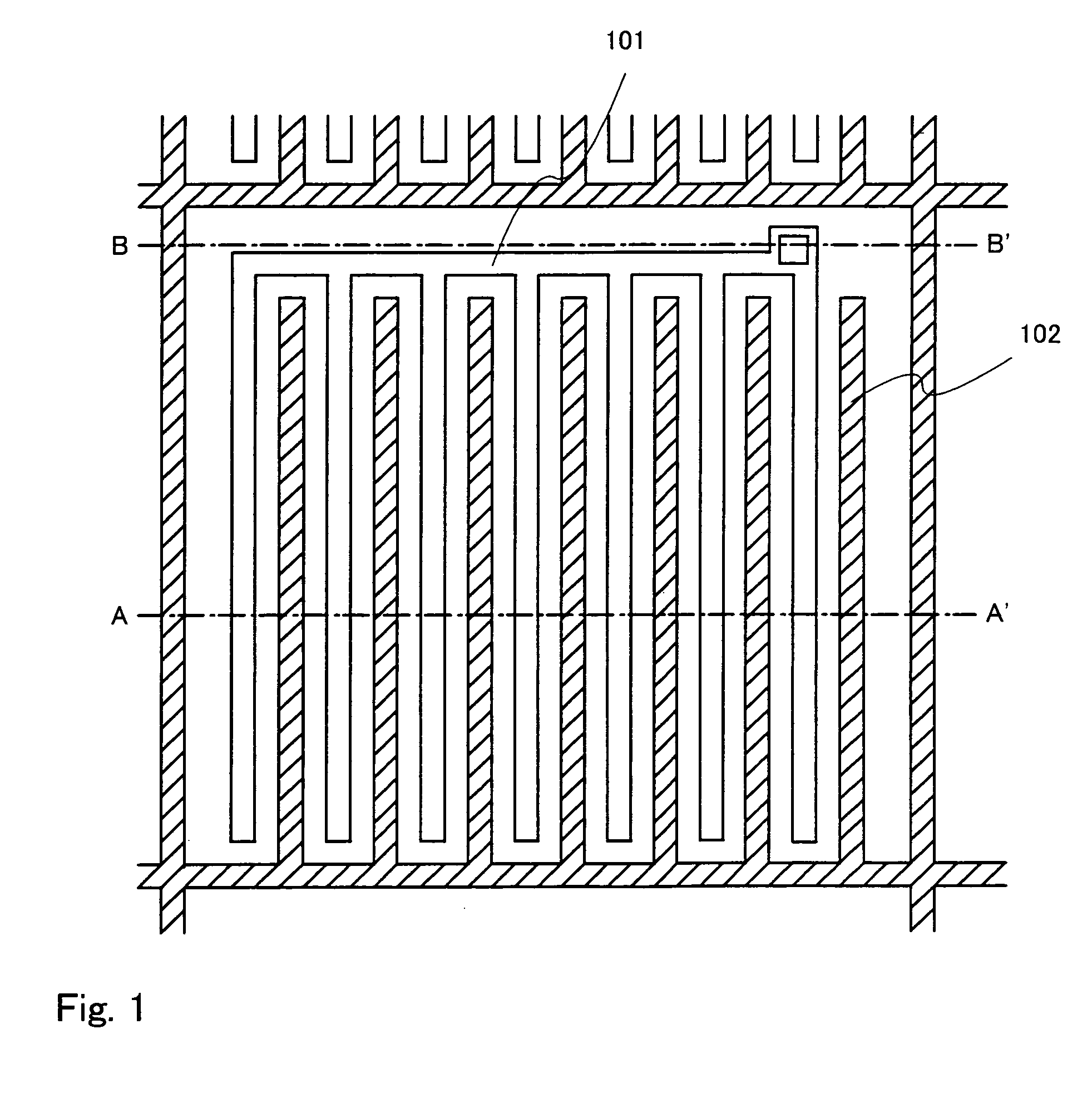
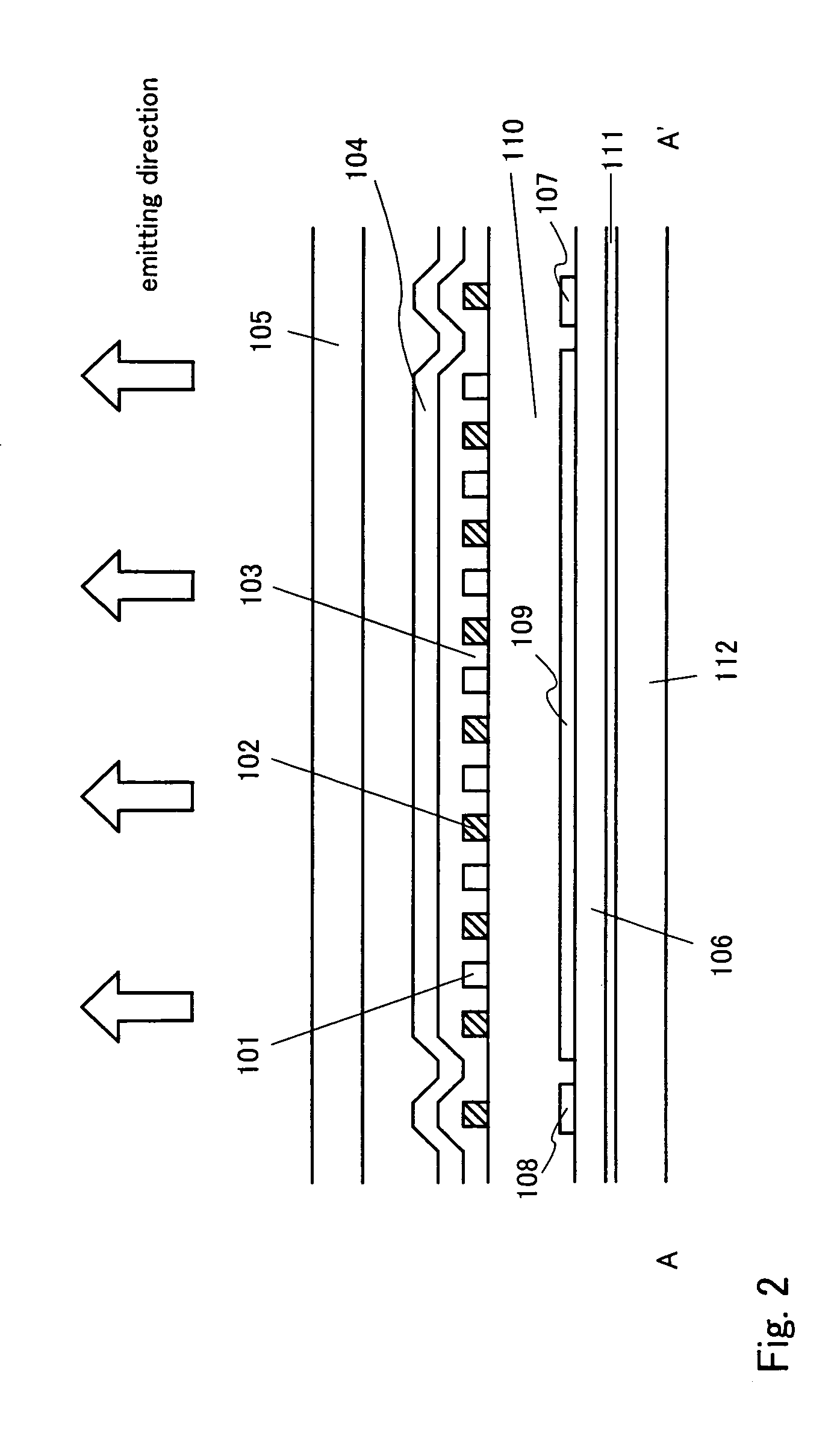
[0029]A light emitting device of the present invention will be described using FIGS. 1 and 2. FIG. 1 is a top view of one pixel provided in the light emitting device. Here, a cross sectional view corresponding to a cross section cut along a line A–A′ in FIG. 1 is shown in FIG. 2 and a cross sectional view corresponding to a cross section cut along a line B–B′ in FIG. 1 is shown in FIG. 9. Note that the same reference symbols are used for the same portions in FIGS. 1, 2, and 9.

[0030]In this embodiment, an active light emitting device will be described.

[0031]In FIG. 2, reference numeral 112 denotes a substrate and reference numeral 111 denotes an insulating film as a base. As the substrate, a silicon substrate, a glass substrate, a quartz substrate, or a plastic substrate is used. When the silicon substrate is used, minute patterning can be performed by using an existing LSI line. Thus, it is preferable to use the silicon substrate. Two or more transistors are provided i...

embodiment 2

[Embodiment 2]

[0047]A light emitting device of the present invention having a structure in which a bipolar layer and a layer containing a luminescent material are laminated as a light emitting layer will be described using FIG. 13. After the cathode and the anode are formed, the bipolar layer is formed. The bipolar a layer is formed by a method described in Embodiment 1. It is required that the film thickness of the bipolar layer is sufficiently smaller than the height of the electrodes. The layer containing the luminescent material is formed on the bipolar layer. As the layer containing the luminescent material, a layer made of one kind of luminescent material or a layer in which the luminescent material is mixed with a mixture made of plural kinds of materials may be used. Thus, when it is viewed along a line C–C′ in FIG. 13, the light emitting element constructed by the anode, the bipolar layer, the layer containing the luminescent material, the bipolar layer, and the cathode can...

embodiment 3

[Embodiment 3]

[0048]A light emitting device in which light is emitted from the lower side of the substrate will be described using FIG. 5. As a substrate 112, a transparent glass substrate, a quartz substrate, or a plastic substrate is used. A reflective film 109 is formed in an upper portion of a light emitting layer 103. The reflective film 109 may be formed over a passivation film 104 or under the passivation film 104. When the reflective film 109 is formed over the passivation film 104, a transparent material is used for the passivation film 104. In this structure, since, of lights produced in the light emitting layer 103, light emitted to the upper side of the substrate is reflected by the reflective film 109, light can be emitted from the lower side of the substrate. Thus, the external quantum efficiency is increased. Another portions are made to be the same structure as Embodiment 1.


PUM


Abstract

In order to emit light from the upper side of a substrate, for example, a treatment is required such that a cathode is thinned. Generally, when light produced in a light emitting layer is passed through the electrode, brightness of a light emitting device is decreased. In the light emitting device of the present invention, an anode and a cathode are located so as to produce an electric field in a direction parallel with the surface of a substrate. Thus, light produced in the light emitting layer is emitted from the lower side or the upper side of the substrate without passing through the electrode.

Description

BACKGROUND OF THE INVENTION[0001]1. Field of the Invention[0002]The present invention relates to a light emitting device employing an element in which a luminescent material is sandwiched between electrodes (hereinafter referred to as a light emitting element), and in particular, a light emitting device employing a luminescent material in which EL (Electro Luminescence) is produced (hereinafter referred to as an EL material).[0003]2. Description of the Related Art[0004]Recently, a development of the light emitting device employing a light emitting element with an EL phenomenon has been progressed. Since the light emitting element itself has luminescent capability, a back light as used in a liquid crystal display device is not required. Further, since the light emitting device has a wide viewing angle, it is suitable for outdoor use.[0005]As the light emitting device, there are two types, that is, a passive type (simple matrix type) and an active type (active matrix type), and both t...

Claims


Application Information

Patent Timeline
Patent Type & Authority Patents(United States)
IPC IPC(8): H05B33/26H05B33/14H01L27/32H01L51/52
CPCH01L51/5203H01L27/3244H01L2251/5315H10K59/12H10K2102/3026H10K59/805H10K50/805
Inventor FUKUNAGA, TAKESHI
Owner SEMICON ENERGY LAB CO LTD
Why Eureka
Try Eureka