

Making contact with semiconductor chips in chip cards
a chip card and semiconductor technology, applied in the field of chip cards, can solve the problems of inability to reliably avoid the damage to the semiconductor chip from this microclimate, the inability of the ambient air to be exchanged with the air in the interior of the second cavity, and the inability to protect the semiconductor chip
- Summary
- Abstract
- Description
- Claims
- Application Information
AI Technical Summary
Benefits of technology
Problems solved by technology
Method used
Image

Examples
Embodiment Construction
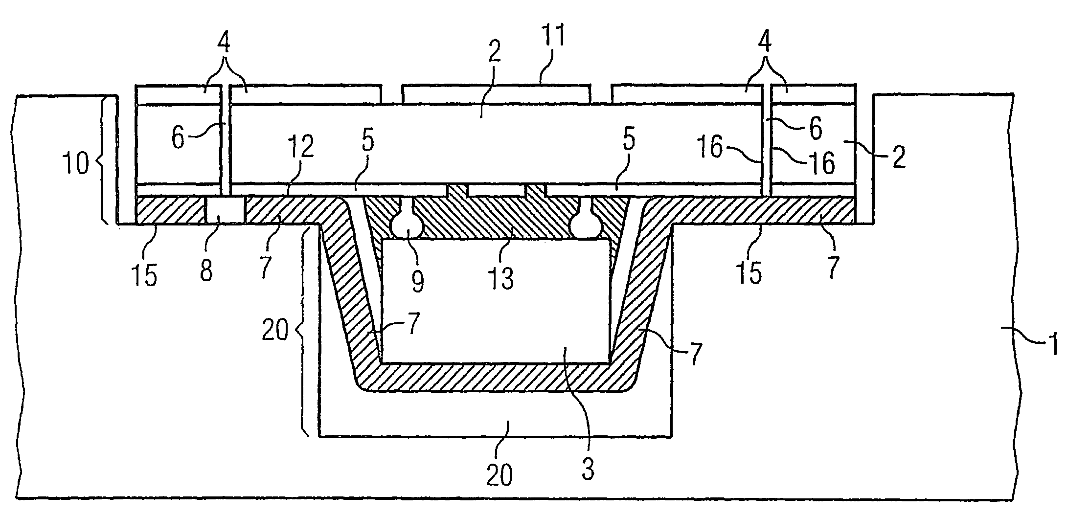
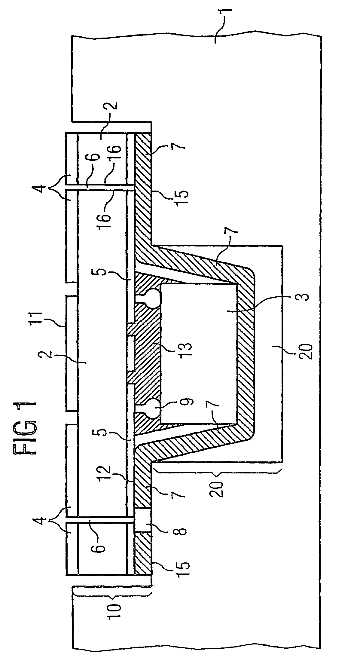
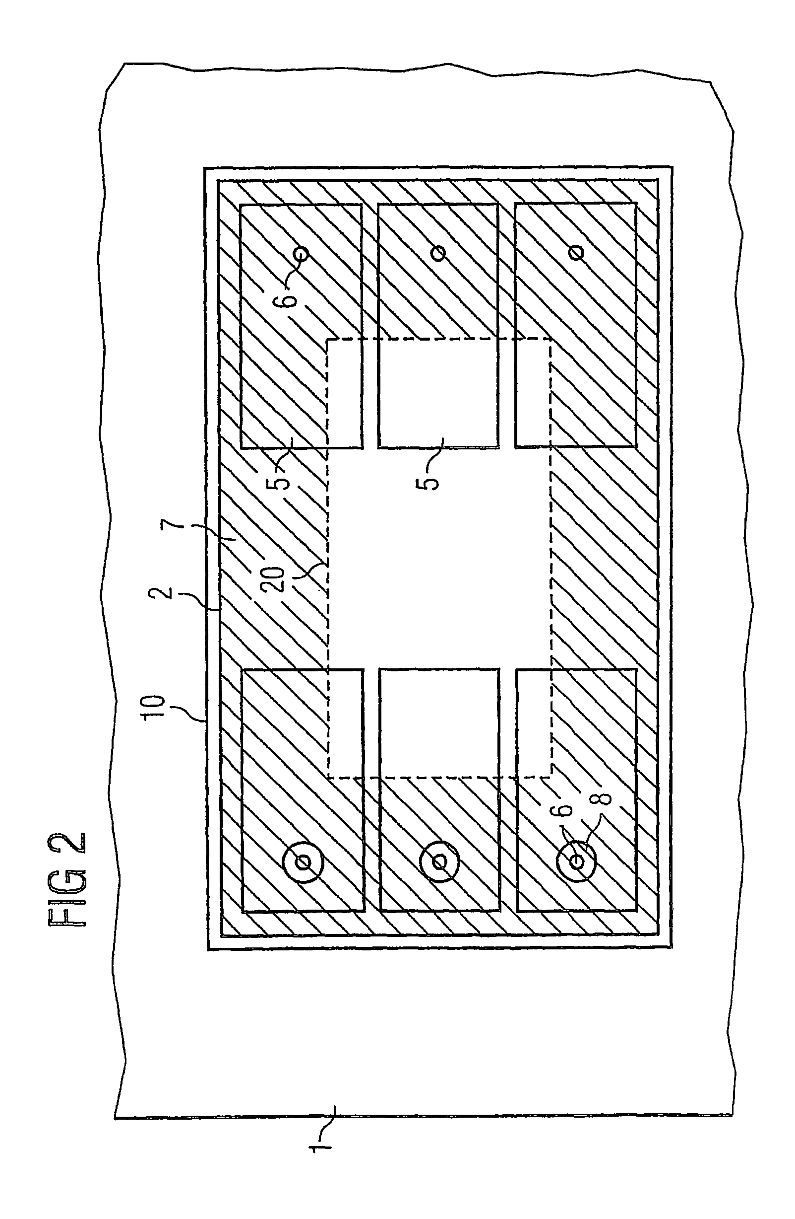
[0028]FIG. 1 shows a chip card body 1, which may consist of a flexible or rigid plastic, in cross section, the thickness of the chip card corresponding to the height of the chip card body 1 illustrated in FIG. 1. The chip card body 1 has an outer cavity 10, which in the lateral direction, i.e., parallel to the chip card surface, has a larger cross section than a further cavity 20, which is recessed into the base 15 of the outer cavity. The outer cavity 10 extends laterally to the left and right and also upward and downward, perpendicular to the plane of the drawing, beyond the inner cavity 20, so that the base surface 15 surrounds the cross section of the inner cavity. In the outer cavity 10 there is a carrier substrate 2. In the inner cavity 20 there is a semiconductor chip 3, which is connected to the carrier substrate 2 by electrical connections 9. The carrier substrate 2 rests on the base surface 15 of the outer cavity 10 via a bonding layer 7 and in this way is secured to the c...
PUM
 Abstract
Description
Claims
Application Information