Method and apparatus for producing a packaged integrated circuit

Inactive Publication Date: 2006-03-28
XILINX INC
View PDF7 Cites 1 Cited by
  • Summary
  • Abstract
  • Description
  • Claims
  • Application Information

AI Technical Summary

Problems solved by technology

However, such conventional systems cannot prevent or detect (i) errors due to wrong setup of the database netlist, (ii) errors created in the artwork mask generation process, or (iii) errors created in subsequent CAD editing processes.
Further, such conventional BGA design systems do not provide for a method of verification once the substrate artwork leaves the original design system.
Furthermore, the availability of the CAD database and/or the textual netlist or pinlist output does not ensure correct verification.
That is, errors in the netlist setup of the database may not be apparent to the reviewer, and the textual netlist output that is generated by the CAD system may not be an accurate representation of the actual design.
Design errors that escape early detection result in huge loss in time to market and costly retooling, which are

Method used


Image

  • Method and apparatus for producing a packaged integrated circuit
  • Method and apparatus for producing a packaged integrated circuit
  • Method and apparatus for producing a packaged integrated circuit

Examples


Example

DETAILED DESCRIPTION OF THE DRAWINGS

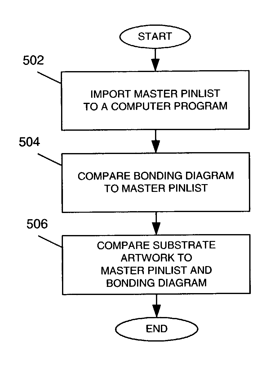
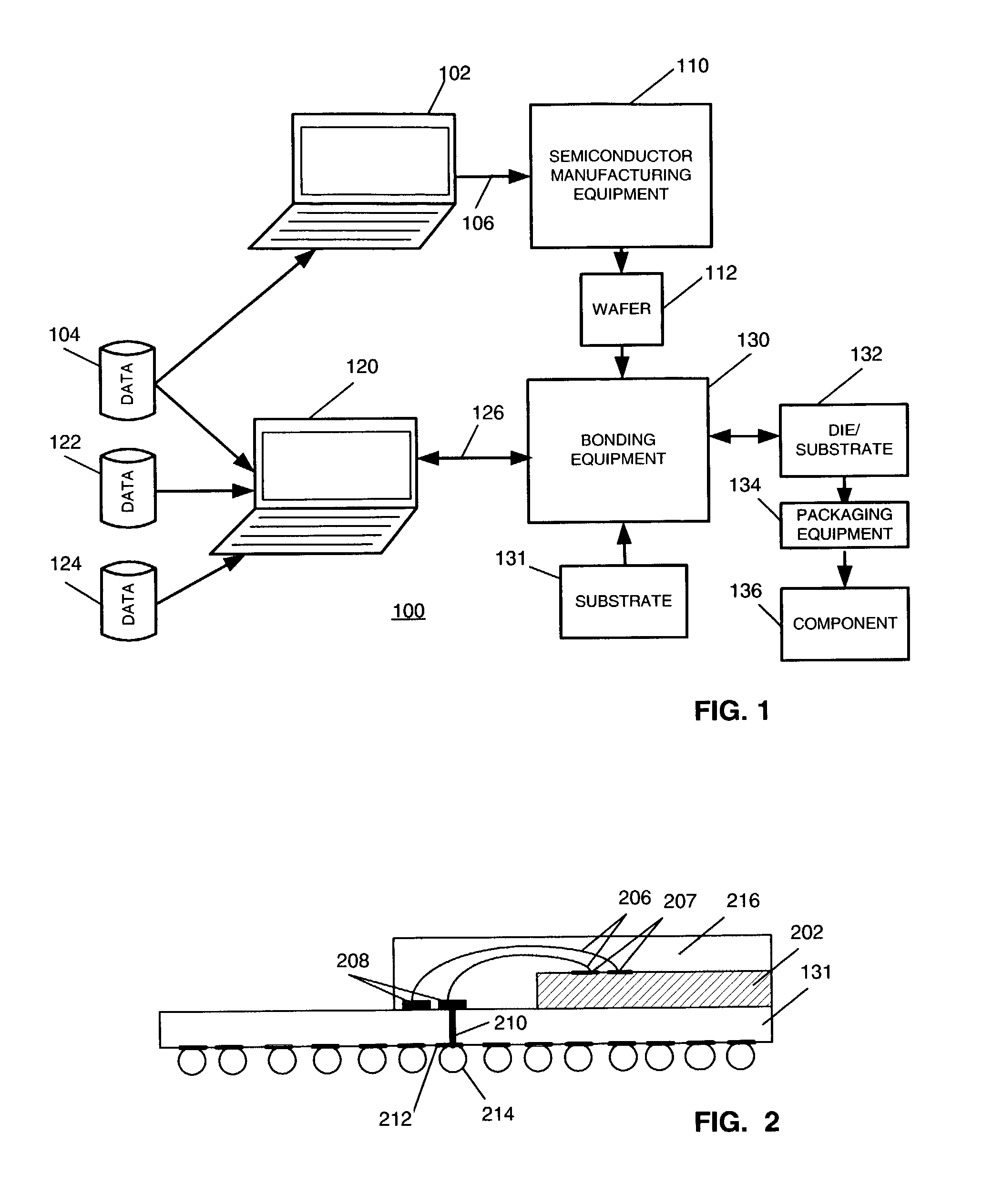
[0023]Turning now to FIG. 1, a block diagram shows a system for designing and manufacturing integrated circuit packages, such as a wirebond BGA, according to the present invention. The system 100 comprises computer aided design (CAD) equipment 102, which could be any computer adapted to run CAD software. The CAD equipment 102 receives data from a master pinlist 104, and is coupled by a communication link 106 to semiconductor manufacturing equipment 110. The communication link 106 could be any wired or wireless communication link. The semiconductor manufacturing equipment 110 generates a wafer 112 having a plurality of die, as is well-known in the art.

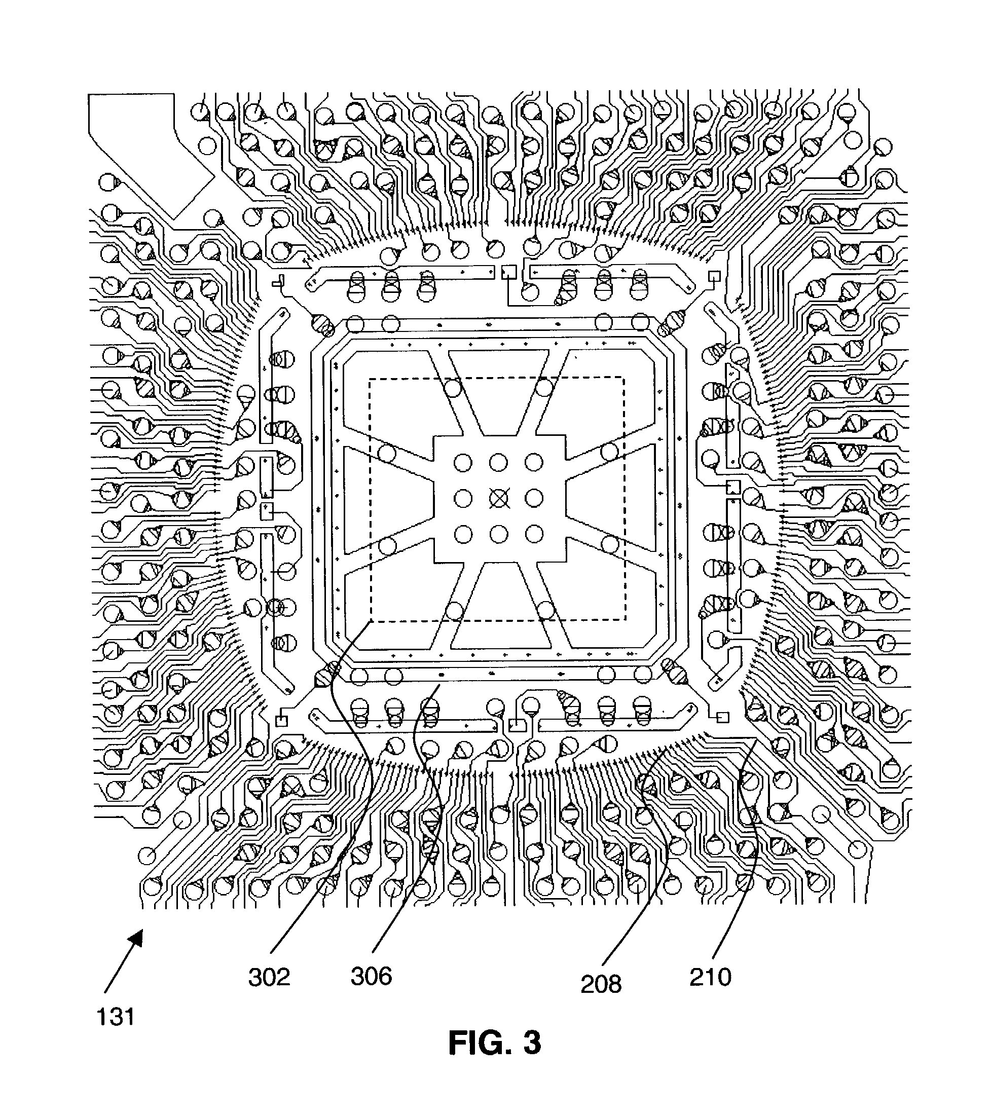
[0024]CAD equipment 120, which is also coupled to receive the master pinlist 104, receives a bonding diagram 122 and substrate artwork 124. The CAD equipment 120 is coupled by a communication link 126 to bonding equipment 130. The communication link could be any wired or wireless communication link. T...


PUM


Abstract

A method of producing a wirebond ball grid array package is described. The method comprises the steps of importing a master pinlist to a computer program, importing a bonding diagram to the computer program, and verifying, by the computer program, substrate artwork against the master pinlist and the bonding diagram. A method of producing a wirebond ball grid array package according to an alternative embodiment comprises the steps of importing a master pinlist to a computer program, importing substrate artwork to the computer program, and verifying, by the computer program, a bonding diagram against the master pinlist and the substrate artwork. Finally, a system for verifying substrate artwork comprises means for importing a master pinlist to a computer program, means for importing a bonding diagram to the computer program, and means for verifying, by the computer program, the substrate artwork against the master pinlist and the bonding diagram.

Description

FIELD OF THE INVENTION[0001]This invention relates generally to packaging integrated circuits, and in particular, to a method and an apparatus for verifying bonding diagrams and substrate artwork during the design and manufacture of a ball grid array package.BACKGROUND OF THE INVENTION[0002]As integrated circuits (ICs) continue to become smaller in size and the circuitry on ICs continues to increase, the number of bonds and the density of the bonds continue to increase. During the manufacture of ICs, silicon wafers having a number of die comprising circuitry are produced according to methods that are well known in the art. A ball grid array (BGA) package is an advanced integrated circuit package comprising a substrate having contacts on the bottom for soldering the integrated circuit package to a circuit board. A BGA package can be formed two ways. A wirebond BGA comprises a die having contact pads which are connected to contact pads on the surface of the substrate by way of wirebon...

Claims


Application Information

Patent Timeline
IPC IPC(8): G06F17/50
CPCG06F17/5068H01L2224/48227H01L2924/15311H01L2224/48091H01L2924/00014G06F30/39
Inventor WU, PAUL YING-FUNG
Owner XILINX INC
Why Eureka
Try Eureka