Memory module having mirrored placement of DRAM integrated circuits upon a four-layer printed circuit board

a technology of integrated circuits and memory modules, which is applied in the field of memory modules with mirrored placement of dram integrated circuits upon a four-layer printed circuit board, can solve the problems of degrading the overall performance and access times of sdram, affecting the performance of memory modules, etc., and achieves the optimization of routing lengths, routing lengths can be shortened, and routing lengths can be optimized.

Active Publication Date: 2006-04-04
AVAGO TECH INT SALES PTE LTD
View PDF17 Cites 36 Cited by
  • Summary
  • Abstract
  • Description
  • Claims
  • Application Information

AI Technical Summary

Benefits of technology

[0013]The problems outlined above are in large part solved by a memory module that can be embedded on the same integrated circuit as the memory controller and the execution unit. Alternatively, the memory module can be configured external to the memory controller or execution unit. An example as an external-configured memory module is one that can plug into a receptacle near the edge of a PCB containing the execution unit and memory controller. An external-configured memory module includes a SIMM or D...

Problems solved by technology

At the relatively high speeds at which data is sent to and from each memory device, any mismatch in trace length between, for example, a controller and the memory devices, will deleteriously affect performance of the memory module.
Thus, lengthy trace conductors a...

Method used


Image

  • Memory module having mirrored placement of DRAM integrated circuits upon a four-layer printed circuit board
  • Memory module having mirrored placement of DRAM integrated circuits upon a four-layer printed circuit board
  • Memory module having mirrored placement of DRAM integrated circuits upon a four-layer printed circuit board

Examples


Embodiment Construction

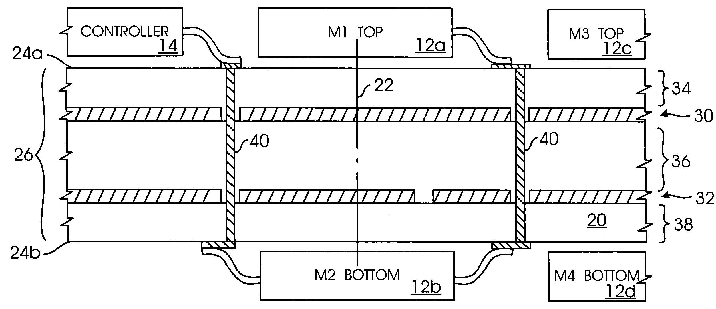
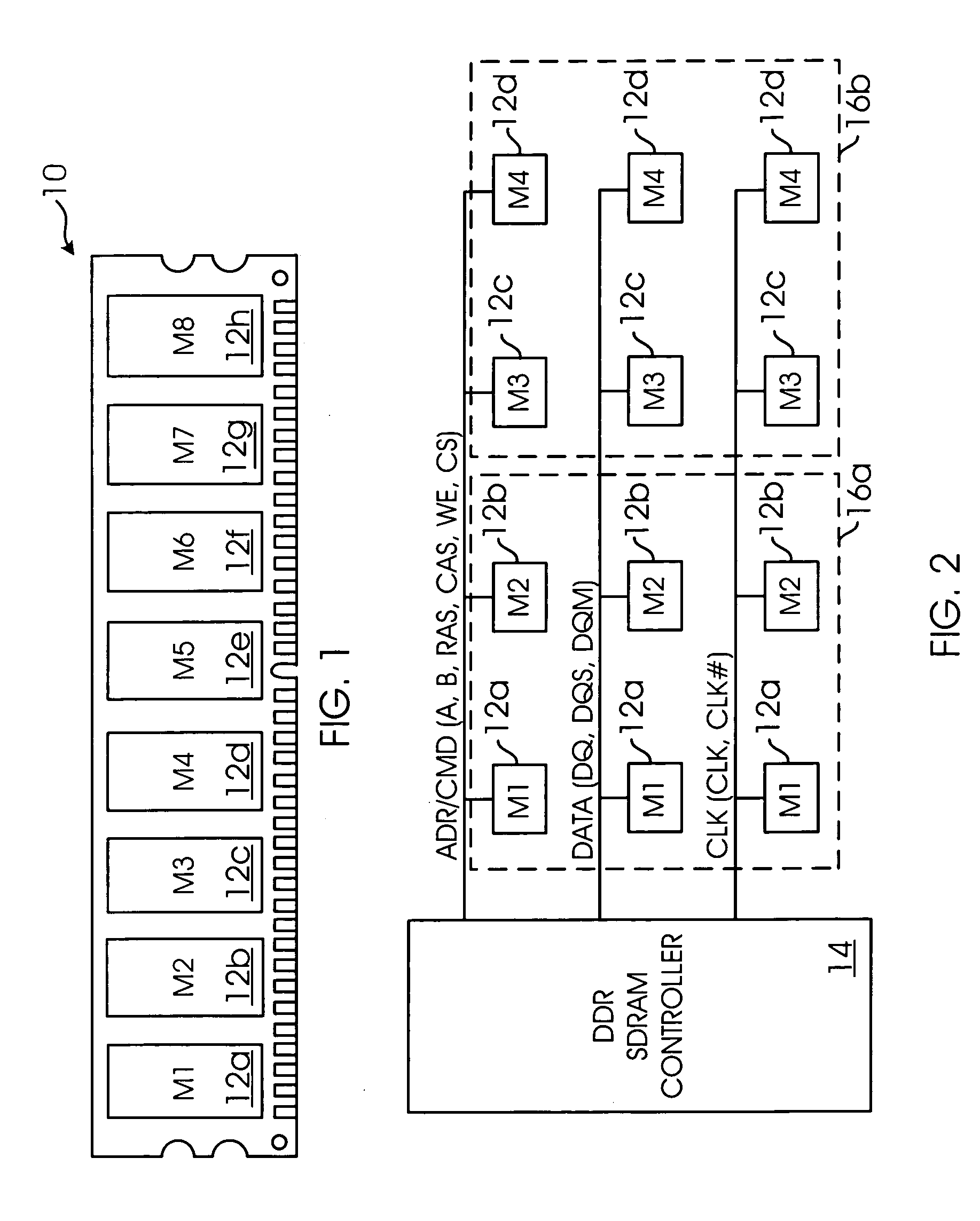
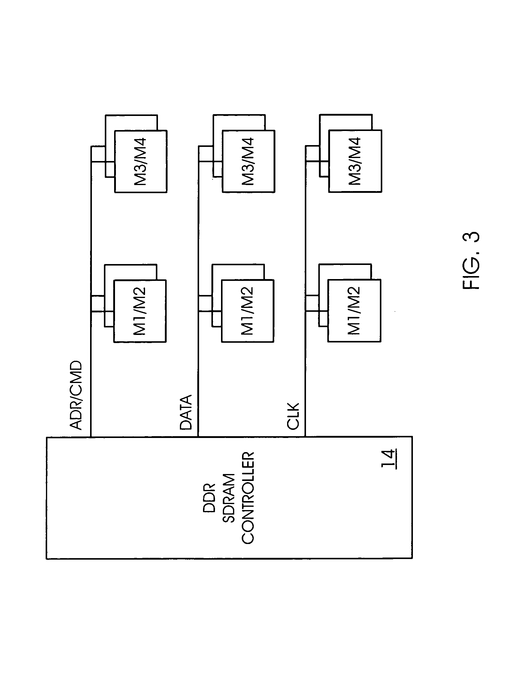
[0029]Turning now to the drawings, FIG. 1 illustrates a memory module 10 having a series of semiconductor memory devices 12 placed on one side of module 10. Each semiconductor memory device is defined as being an individual die taken from a semiconductor wafer and hermetically sealed inside a package. The package includes leads that extend from an outer surface of the package, and the leads can thereafter be forwarded through holes or affixed to conductors on the surface of a card or board. There are various types of packages, some of which are through-hole packages and others being surface-mounted packages. Distinguishable from packages which have leads that extend downward into plated holes within a card, surface-mounted packages have leads which extend either flush with the outer surface of the package or outward, flush with a bottom surface of the package. In the latter instance, leads which extend outward are often referred to as a quad flat package (QFP) or a small outline pac...


PUM


Abstract

A memory module is provided as well as a method for forming a memory module. The memory module includes a printed circuit board having opposed first and second outside surfaces. At least one via can extend through the printed circuit board and couples a conductor on one outside surface to a conductor on another outside surface. A semiconductor memory device on one of those outside surfaces can thereby be connected to one end of the via, with another semiconductor memory device on the opposing outside surface connected to the other end of the via. Preferably, the pair of memory devices are placed on a portion of each respective outside surface so that they essentially align in mirrored fashion with each other. Accordingly, any vias which extend from the footprint of one memory device will take the shortest path to the footprint of the other memory device, with the stubs between the footprint and the via being of essentially the same length and relatively short. The printed circuit board preferably has no more than four conductive layers dielectrically spaced from each other. Two layers are reserved for the opposing outer surfaces, and two layers carrying power and ground signals are embedded within the board. The memory devices are preferably DDR SDRAMs connected to each other as well as a memory controller, each of are placed and maintained upon a single printed circuit board.

Description

BACKGROUND OF THE INVENTION[0001]1. Field of Invention[0002]This invention relates to semiconductor memory and, more particularly, to packaged semiconductor memory placed in slots that mirror each other on opposing sides of a four layer printed circuit board to optimize the inter-memory and controller-to-memory routing lengths.[0003]2. Description of Related Art[0004]The following descriptions and examples are not admitted to be prior art by virtue of their inclusion within this section.[0005]There are numerous types of memories available in the marketplace. For example, large volumes of data can be stored in magnetic memory, such as a hard disk drive. Lesser quantities of data can be stored in memory arranged upon an integrated circuit, oftentimes referred to as “semiconductor memory.” Semiconductor memory is typically arranged closer to the core logic unit or execution unit than the hard disk drive and can be accessed much faster than the disk drive.[0006]Common to semiconductor m...

Claims


Application Information

Patent Timeline
IPC IPC(8): G11C5/06
CPCG11C5/04H05K1/181G11C5/063H05K2201/10545Y02P70/50
Inventor HUNG, ERICSAI, NORMAN
Owner AVAGO TECH INT SALES PTE LTD
Why Eureka
Try Eureka