Gate dielectric antifuse circuits and methods for operating same

a dielectric and gate dielectric technology, applied in the field of integrated circuits, can solve the problems of limited use of antifuses in integrated circuits and the inability of polysilicon fuses to be opened once, and achieve the effect of reducing current flow and reducing leakage curren

Inactive Publication Date: 2006-04-18
MICRON TECH INC
View PDF44 Cites 29 Cited by
  • Summary
  • Abstract
  • Description
  • Claims
  • Application Information

AI Technical Summary

Problems solved by technology

In addition, polysilicon fuses cannot be opened once an integrated circuit is placed in an integrated circuit package, or is encapsulated in any manner.
Despite their advantages, the use of antifuses in integrated circuits is limited by a lack of adequate circuitry to support the programming and reading of the antifuses.

Method used


Image

  • Gate dielectric antifuse circuits and methods for operating same
  • Gate dielectric antifuse circuits and methods for operating same
  • Gate dielectric antifuse circuits and methods for operating same

Examples


Embodiment Construction

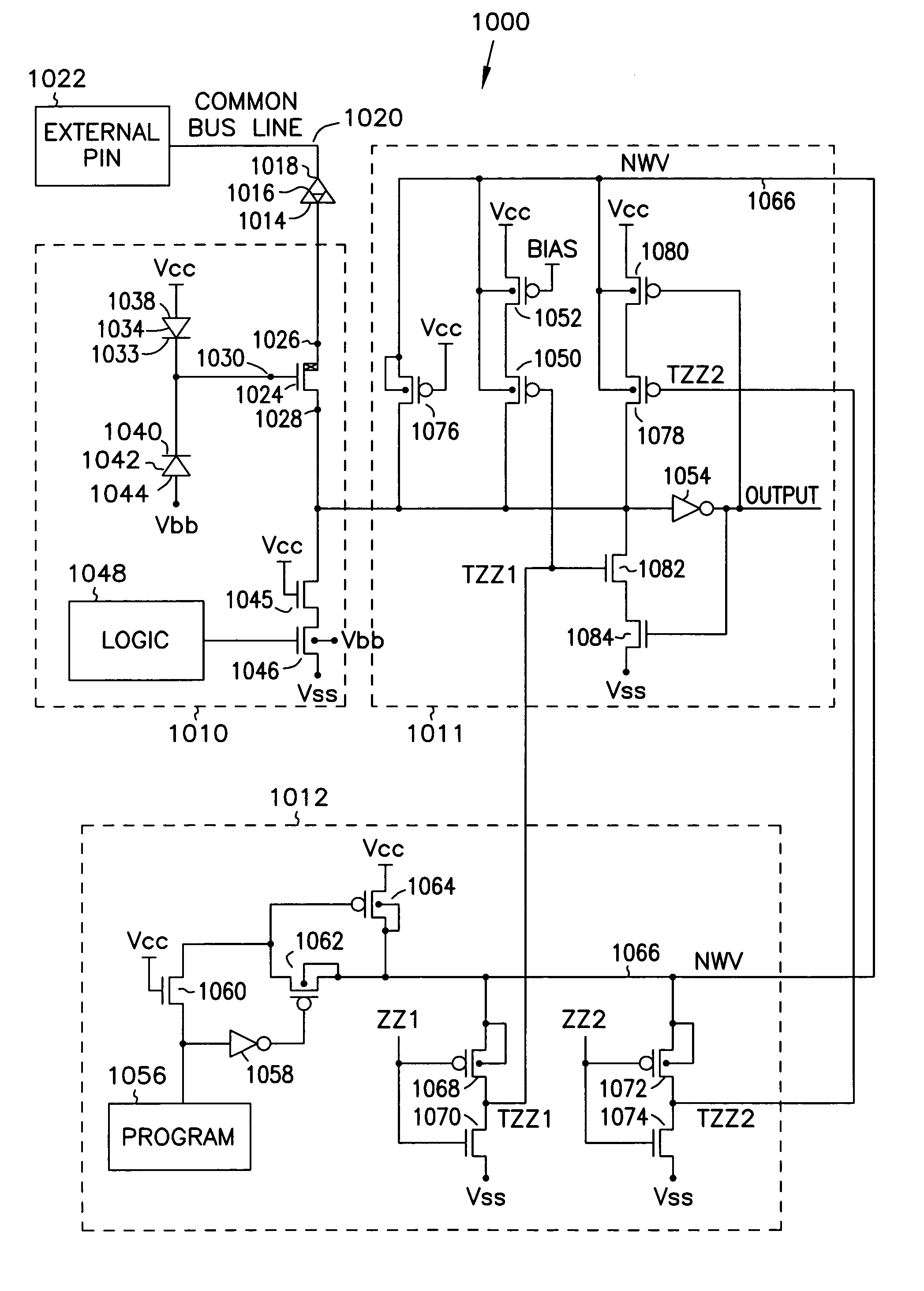
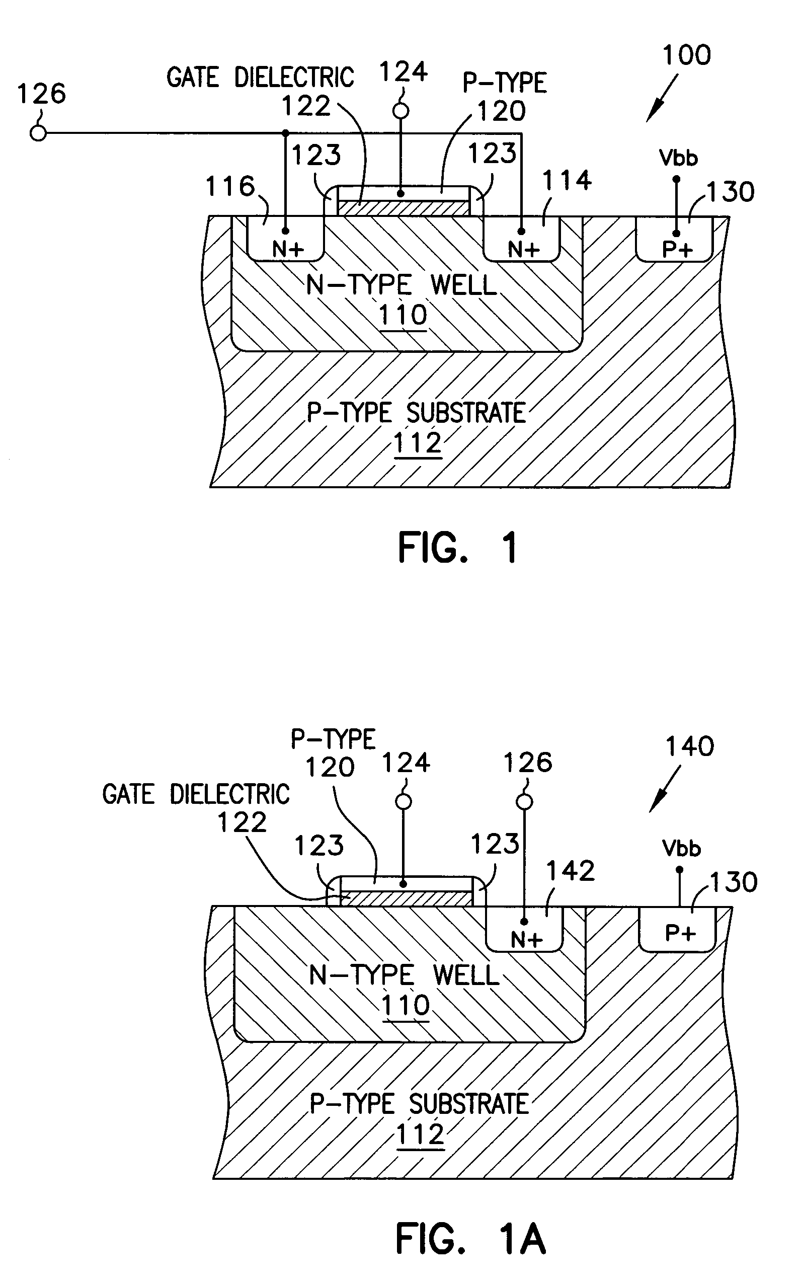
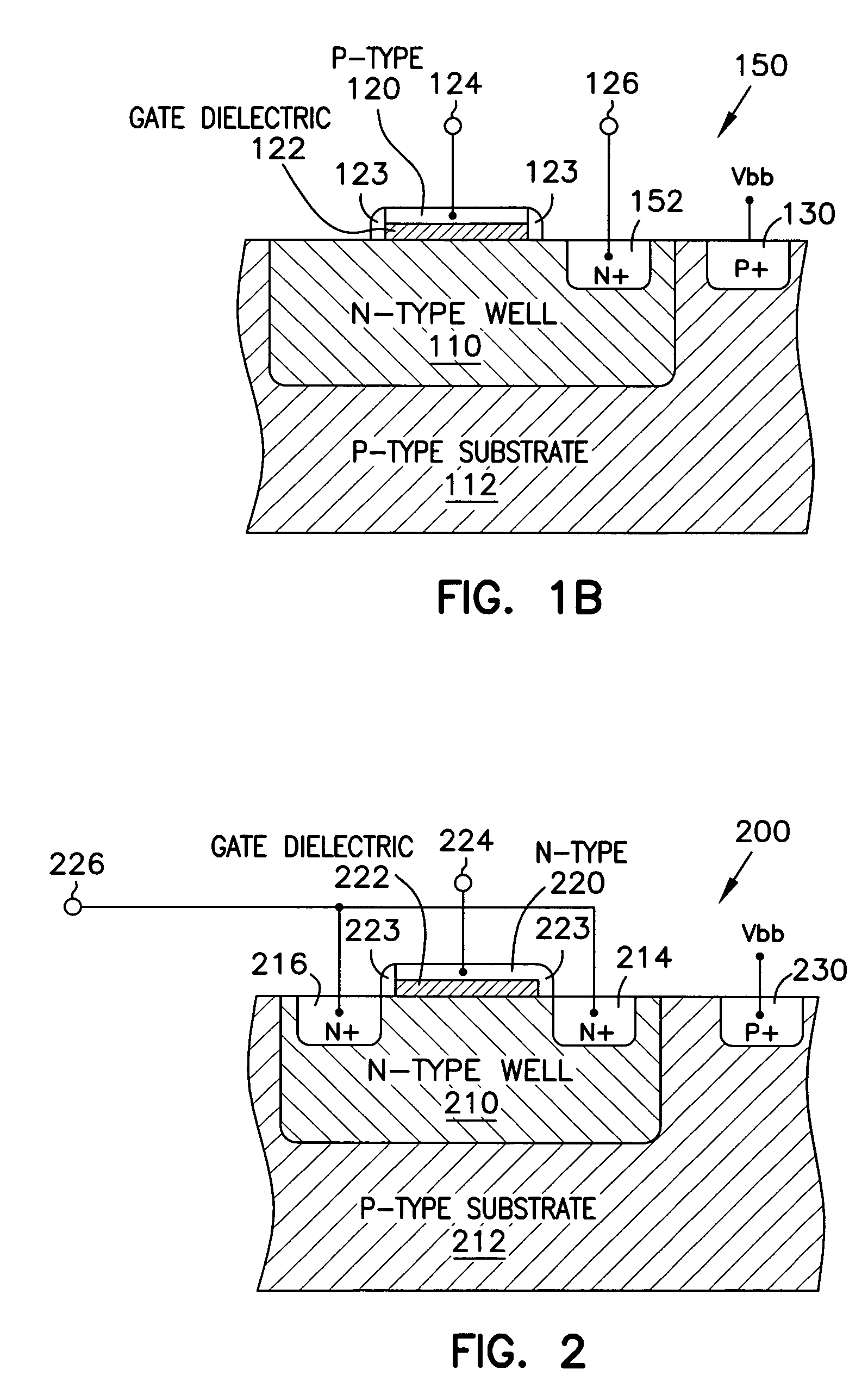
[0045]In the following detailed description of exemplary embodiments of the present invention, reference is made to the accompanying drawings which form a part hereof, and in which are shown by way of illustration specific exemplary embodiments in which the present invention may be practiced. These embodiments are described in sufficient detail to enable those skilled in the art to practice the present invention, and it is to be understood that other embodiments may be utilized and that logical, mechanical, electrical and other changes may be made without departing from the spirit or scope of the present invention. The following detailed description is, therefore, not to be taken in a limiting sense, and the scope of the present invention is defined only by the claims.

[0046]The terms wafer and substrate may be used in the following description and include any structure having an exposed surface with which to form an integrated circuit (IC) according to embodiments of the present inv...


PUM


Abstract

A number of antifuse support circuits and methods for operating them are disclosed according to embodiments of the present invention. An external pin is coupled to a common bus line in an integrated circuit to deliver an elevated voltage to program antifuses in a programming mode. An antifuse having a first terminal coupled to the common bus line is selected to be programmed by a control transistor in a program driver circuit coupled to a second terminal of the antifuse. The program driver circuit has a high-voltage transistor with a diode coupled to its gate to bear a portion of the elevated voltage after the antifuse has been programmed. The program driver circuit also has an impedance transistor between the high-voltage transistor and the control transistor to reduce leakage current and the possibility of a snap-back condition in the control transistor. A read circuit includes a transistor coupled between a read voltage source and the second terminal to read the antifuse in an active mode. The common bus line may be coupled to a reference voltage through a common bus line driver circuit in the active mode to pass current to or from the read circuit. The common bus line driver circuit has a control transistor and a high-voltage transistor with a diode coupled to its gate to bear the elevated voltage on the common bus line during the programming mode. The read circuit may have a latch circuit to latch a state of the antifuse in a sleep mode. A floating well driver logic circuit raises the voltage potential of wells and gate terminals of p-channel transistors in the read circuit during the programming mode to reduce current flow from the common bus line.

Description

[0001]This application is a divisional of U.S. application Ser. No. 09 / 652,429 filed on Aug. 31, 2000, now U.S. Pat. No. 6,630,724, which is incorporated herein by reference.FIELD OF THE INVENTION[0002]The present invention relates generally to integrated circuits, and more particularly, to antifuse circuits and methods for operating them.BACKGROUND[0003]Integrated circuits are interconnected networks of electrical components fabricated on a common foundation called a substrate. The electrical components are typically fabricated on a wafer of semiconductor material that serves as a substrate. Various fabrication techniques, such as layering, doping, masking, and etching, are used to build millions of resistors, transistors, and other electrical components on the wafer. The components are then wired together, or interconnected, to define a specific electrical circuit, such as a processor or a memory device.[0004]Fusible elements are employed in integrated circuits to permit changes i...

Claims


Application Information

Patent Timeline
Patent Type & Authority Patents(United States)
IPC IPC(8): H01L29/00G11C17/16G11C17/18H01L23/525
CPCG11C17/16G11C17/165G11C17/18G11C29/02G11C29/027H01L23/5252H01L27/1203H01L29/66659H01L29/7835H01L2924/3011H01L2924/0002H01L2924/00
Inventor MARR, KENNETH W.
Owner MICRON TECH INC
Why Eureka
Try Eureka