
Four-terminal methods for resistivity measurement of semiconducting materials

a semiconducting material and resistivity measurement technology, applied in the direction of electrical testing, instruments, electrical apparatus, etc., can solve the problems of increasing the difficulty of device engineers designing and simulating device structures, affecting the accuracy of semiconductor resistivity measurement, etc., to achieve accurate measurement of semiconductor resistivity of thin films, reduce contact resistance, and evaluate resistivity uniformity

Inactive Publication Date: 2006-04-18
XIAO STEVEN SHUYONG
View PDF4 Cites 33 Cited by
  • Summary
  • Abstract
  • Description
  • Claims
  • Application Information

AI Technical Summary

Benefits of technology

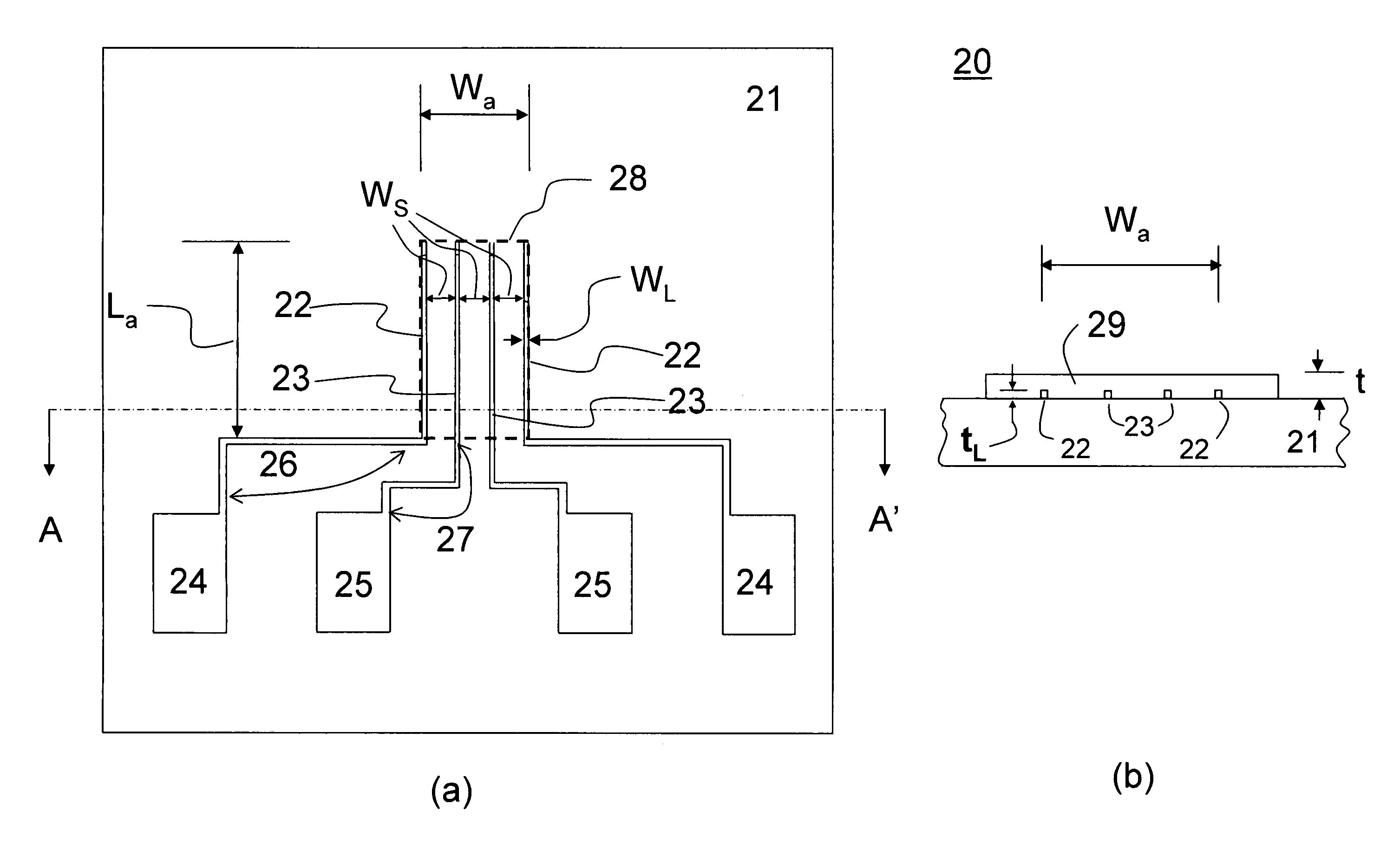
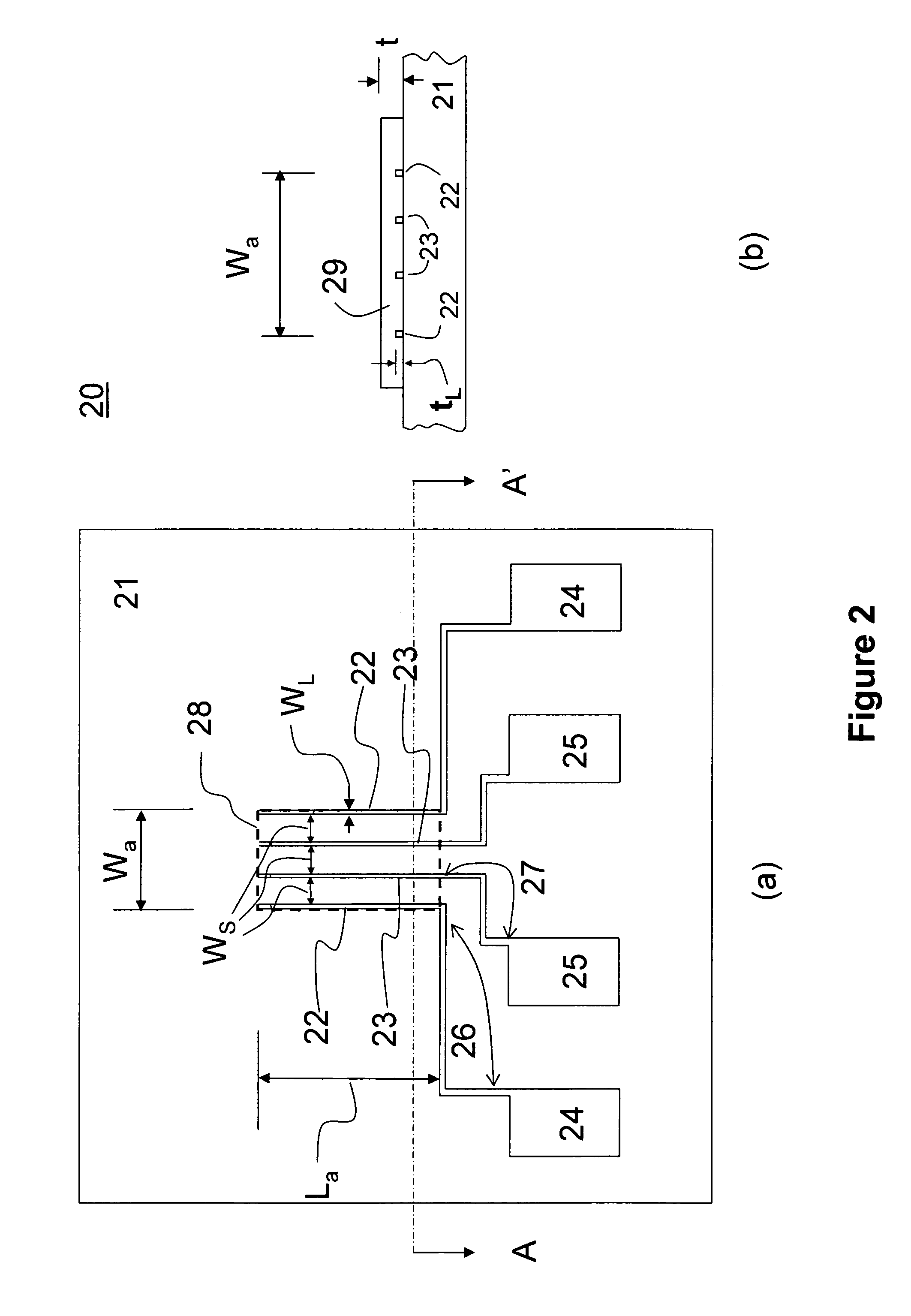
[0009]One objective of this invention is to disclose four-line structures for standardized resistivity measurement of semiconductors. One other objective is to disclose multi-line structures for resistivity measurement of semiconductors. Another objective is to provide a four-terminal method to accurately measure resistivity of semiconductor thin films using the four-line and the multi-line structures. Still another objective is to provide methods to evaluate resistivity uniformity of semiconductor thin films using the multi-line structures. Yet another objective is to provide means to reduce the contact resistance between the conducting lines in the structures and the semiconductors.

Problems solved by technology

Unfortunately, the electrical conductivity values reported by material manufactures vary widely from the actual values, caused by lack of a standardized resistivity measurement method.
These added uncertainties will make it more difficult for the device engineers to design and simulate device structures.
It is almost impossible to determine the resistivity of an organic semiconductor in chunks.
For polymers in liquid form, because most of undoped polymers are not good conductors, it is rather difficult to accurately measure the resistivity of polymers in a liquid.
Furthermore, the resistivity values of polymers quoted at different concentration and dissolved in different solvents also add confusion in the already vague specification sheet of conducting polymers.
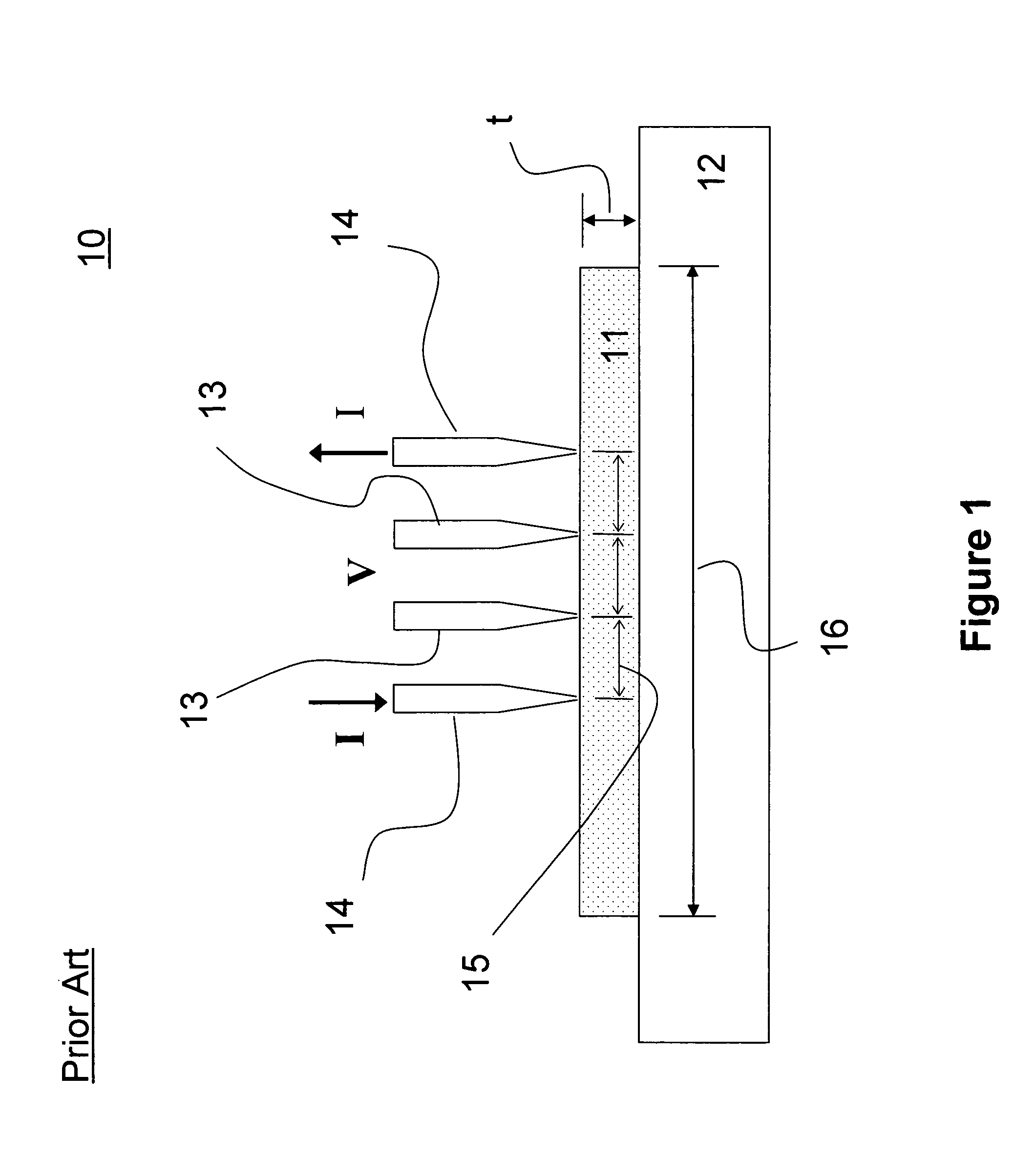
However, due to the large resistivity of undoped organic semiconducting materials and high contact resistance presenting between the metal probes and the thin organic films, the current that can pass through an organic semiconducting film through the needle probes is extremely small and not easy to measure, hence, the traditional four-point probe method ceases to be an effective way of evaluating the resistivity of an organic semiconducting film.

Method used


Image

  • Four-terminal methods for resistivity measurement of semiconducting materials
  • Four-terminal methods for resistivity measurement of semiconducting materials
  • Four-terminal methods for resistivity measurement of semiconducting materials

Examples


examples

[0064]In the following examples we present resistivity measurement results for some typical organic semiconductors using the four-line structure and the four-terminal measurement methods.

1. Four-Line Testing Chip

[0065]The four-line structure testing chips used in the examples are fabricated on glass slides but one should not limit oneself to glass substrates only.

[0066]Four-line testing chip parameters used in the examples are:[0067]Substrate: glass slide[0068]Substrate dimension: 1.1×1.1 cm2 [0069]Substrate thickness: 1 mm[0070]Metallic liner length: 3.5 mm[0071]Metallic line width: 3.0 μm[0072]Spacing between fingers: 50 μm[0073]Metals used: Au, Ag, Ti, Al[0074]Resistance of metallic lines: <1 ohm

2. Four-Terminal Resistivity Measurement

[0075]In this section, we will give a few examples of four-terminal resistivity measurements carried out on several typical organic semiconductor materials. In this work, we have employed a Hewlett Packard DC power supply (mode no. 6200B) and two HP...


PUM


Abstract

This invention provides an innovative multi-line structure and an effective four-terminal method for the resistivity measurement of semiconductor materials. The multi-line structure and the four-terminal method not only allow one to perform resistivity measurement on any inorganic and organic semiconductor thin film conveniently, rapidly and accurately but also offer the means to study resistivity uniformity across the semiconductor thin film.

Description

FIELD OF THE INVENTION[0001]This invention relates to methods to characterize semiconductors in general and organic semiconducting materials in particular for electronic and optoelectronic applications. More specifically, it relates to multi-line structures and four-terminal measurement methods for standardized resistivity measurements of semiconducting materials, and the method to prepare the multi-line structures.BACKGROUND OF THE INVENTION[0002]The discovery of metal-like electrical properties of polyacetylene when exposed to oxidizing agents like iodine vapor in 1977 by Shirakawa, Heeger and MacDiarmid introduced of a group of new members into the semiconductor family—the organic semiconductors and earned the discoverers the Nobel Prize for chemistry in the year 2000. This discovery created a tremendous opportunity as the organic semiconductors exhibit a combination of properties of metals and plastics, being conductive and flexible at the same time. Since then, efforts of the i...

Claims


Application Information

Patent Timeline
IPC IPC(8): G01R31/26
CPCG01N27/045H01L22/14G01R31/2884G01R31/2648
Inventor QIU, CHUNONGQIU, CINDY X.XIAO, STEVEN SHUYONG
Owner XIAO STEVEN SHUYONG
Learn More