Error detector, semiconductor device, and error detection method

Inactive Publication Date: 2006-04-18
SOCIONEXT INC
View PDF11 Cites 3 Cited by
  • Summary
  • Abstract
  • Description
  • Claims
  • Application Information

AI Technical Summary

Benefits of technology

[0064]In another aspect of the present invention, in the error detection method, each of the first buffer unit for receiving the remainder from the first division procedure and the second buffer unit for receivin

Problems solved by technology

As a result, the reception bit string can be judged to be erroneous if the value of the register unit when the feedback shift register has

Method used


Image

  • Error detector, semiconductor device, and error detection method
  • Error detector, semiconductor device, and error detection method
  • Error detector, semiconductor device, and error detection method

Examples


first embodiment

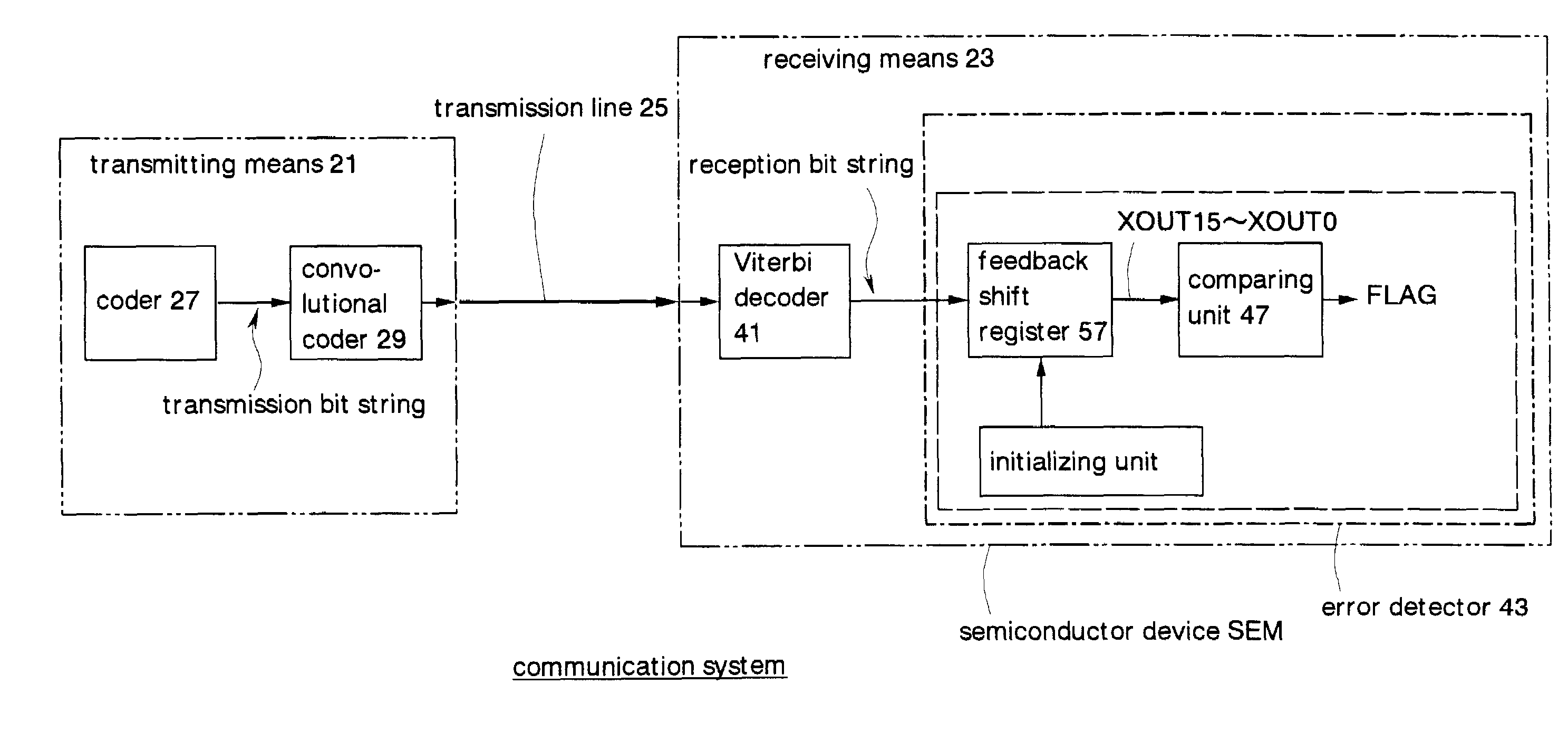
[0096]FIG. 6 is a block diagram showing the basic principle of an error detector, a semiconductor device comprising the error detector, and an error detection method according to the present invention. Transmitting means and receiving means corresponding respectively to a transmitter 21 and a receiver 23, which will be described later, are connected to each other via a transmission line corresponding to a radio transmission line 25. The transmitting means, the receiving means, and the transmission line constitute the communication system.

[0097]The transmitting means comprises a coder 27 and a convolutional coder 29, which will be described later. The receiving means comprises a decoder corresponding to a Viterbi decoder 41, which will be described later, and an error detector 43.

[0098]The error detector 43 is composed of, e.g., a semiconductor device SEM, and comprises a feedback shift register 45 and a comparing unit 47, each of which will be described later.

[0099]The transmitting ...

fourth embodiment

[0214]Although the:fourth embodiment has described the example in which the error detection is performed by shifting each of the first and second feedback shift registers 67 and 69 from “STATE 0” to “STATE 11” and comparing the respective values held by the F / F circuits X15 to X0 in “STATE 11”, the present invention is not limited to such an embodiment. For example, the error detection may also be performed by shifting the first feedback shift register 67 to “STATE 15” and the second feedback shift register 69 to “STATE 7” and comparing the first feedback shift register 67 in “STATE 15” and the second feedback shift register 69 in “STATE 7”. In short, the first feedback shift register 67 according to such an embodiment undergoes transitions from “STATE O” to “STATE 22” in FIG. 27. The second feedback shift register 69 undergoes transitions from “STATE 22” to “STATE 0” in FIG. 27. Consequently, the respective “states” of the first and second feedback shift registers 67 and 69 come to...


PUM


Abstract

An error detector at a receiver comprises a feedback shift register. A shift direction in the feedback shift register is opposite to a shift direction at a transmitter in generating a transmission bit string by using a specified generator polynomial. A reception bit string is inputted to the feedback shift register in reverse order to the transmission bit string was generated at the transmitter so that errors in the reception bit string is detected by obtaining the remainder. Another error detector at a receiver comprises first and second feedback shift registers. Respective shift directions in the first and second feedback shift registers are the same as and opposite to a shift direction at a transmitter in generating a transmission bit string. The reception bit string is inputted to the first feedback shift register in the same order in which the transmission bit string was generated, while the reception bit string is inputted to the second feedback shift register in reverse order to one which the transmission bit string was generated. Errors in the reception bit string are detected by comparing respective remainders obtained by the first and second feedback shift registers. This reduces the processing time required for the error detection and increases efficiency in detecting errors in transmitted data.

Description

CROSS-REFERENCE INFORMATION[0001]This is a Division of prior application Ser. No. 09 / 311,722, filed May 14, 1999, now U.S. Pat. No. 6,493,844 B1. The disclosure of the prior application is hereby incorporated by reference herein in its entirety.BACKGROUND OF THE INVENTION[0002]1. Field of the Invention[0003]The present invention relates to a detection of errors in data and, more particularly, to an error detector for detecting errors that occur in data under transmission.[0004]The present invention relates to a semiconductor device comprising the error detector.[0005]The present invention relates to an error detection method for detecting errors that occur in data under transmission.[0006]2. Description of the Related Art[0007]There are various factors which may cause errors in data being transmitted via transmission lines. For the detecting the errors, a transmitter in a communication system adds check data, under a given rule, to target data to be transmitted. A receiver in the co...

Claims


Application Information

Patent Timeline
IPC IPC(8): H03M13/00H03M13/23H04L1/00
CPCH03M13/09H03M13/091H03M13/41H03M13/39H03M13/23H04L1/00
Inventor KANASUGI, MASAMITANIGUCHI, SHOJIKUROIWA, KOICHIHIKITA, MAHIRO
Owner SOCIONEXT INC
Why Eureka
Try Eureka