Combination SD/MMC flash memory card with thirteen contact pads

a technology of contact pads and memory cards, which is applied in the direction of printed circuits, programmable/customizable/modifiable circuits, instruments, etc., can solve the problems of sd cards, inability to fit in mmc slots, etc., and achieve the effect of convenient and inexpensive production and efficient integrated sd/mmc host systems

Inactive Publication Date: 2006-04-25
SUPER TALENT ELECTRONICS
View PDF28 Cites 50 Cited by
  • Summary
  • Abstract
  • Description
  • Claims
  • Application Information

AI Technical Summary

Benefits of technology

[0009]The present invention is directed to a 13-pad memory card including a printed circuit board assembly (PCBA) that is consistent with existing 13-pad MMC mechanical form factors, and a housing that is consistent with the SD mechanical form factor. In particular, the PCBA includes thirteen contact pads arranged in a pattern consistent with MMC Specification Version 4.0 mechanical form factors, and the housing includes both upper and lower covers that mount over the upper and lower surfaces of the PCBA. By packaging the MMC-compliant PCBA in the SD-type housing in the manner described herein, the present invention facilitates an efficient integrated SD / MMC host system that recognizes and communicates with memory cards operating on either SD or MMC electronic protocols. The present invention also facilitates the inexpensive production of both SD and / or MMC memory cards for the integrated SD / MMC host system because the PCBA and housing assembly can be utilized to produce cards of both types.
[0010]According to an embodiment of the present invention, the PCBA includes a printed circuit board (PCB) having a 13-pad contact pad array formed on an upper surface thereon, and one or more integrated circuits (e.g., a controller and a flash memory chip) mounted on a lower surface thereof. The thirteen contact pads of the array are arranged in a manner that complies with the MMC Specification Version 4.0 form factor, but includes at least one reduced-size contact pad to facilitate the inclusion of a write protect switch on the housing, which is needed to comply with the SD mechanical form factor. In particular, the elongated C8 contact pad of MMC Specification Version 4.0 is shortened such that its back end is aligned with the other contact pads arranged along the front edge of the PCBA. This shortened contact pad facilitates the formation of an alignment notch that mounts over a write protect switch mounting structure formed on the housing. During assembly, the write protect switch mounting structure is received inside the alignment notch, thereby maintaining the PCBA in a proper orientation inside the housing. An optional write protect switch is slidably inserted into the write protect switch structure (note that the slidable switch structure may be omitted in MMC versions of the memory card). Accordingly, a PCBA and housing assembly is provided that can be used to manufacture either SD or MMC memory cards (i.e., by mounting ICs that execute the corresponding SD or MMC protocol), thereby reducing manufacturing costs by avoiding the need to produce multiple housings and / or PCBAs.
[0011]In one embodiment, the PCBA is mounted in a housing including upper and lower covers that are joined at a seam that located inboard of one of the side walls. This internal joining beneficially prevents bonding material from overflowing to the exterior of the apparatus, and also minimizes the chances of misalignment between the upper and lower covers (and at the same time eliminating the need for high-precision alignment tooling for assembly). In addition, since the sides of the card-type electronic apparatus can be formed from just the sidewalls of the lower cover (rather than from a combination of sidewalls from both the upper and lower covers), control over the dimensional integrity of the apparatus can be more easily maintained.
[0012]In another embodiment, the interior surfaces of the housing covers are formed with a slight angle (i.e., such that the thickness of the cover gradually changes between the front and back edges of the housing), thereby maintaining the PCBA at an inclined angle relative to the outer cover surface (i.e., such that the exposed contact pads are tilted slightly down in the leading edge). The SD mechanical form factor requires that the contact pads be maintained at a specific distance (0.7 mm) from the top of the housing, and that the overall housing thickness is limited to 2.1 mm. Forming the housing such that the PCBA is maintained at a slightly angled orientation produces two benefits. First, by making the upper cover thinner near the trailing edge of the housing, the trailing edge of the PCBA can be raised relative to the front edge. As a result, a larger vertical space is provided inside the housing for the ICs (i.e., relative to a horizontal PCBA orientation), thereby allowing the use of relatively thick flash memory chips (e.g., a Thin Small Outline Package (TSOP) package with a thickness of 1.1 mm). Second, because the contact pads are slightly tiled, as the contact pads are received in a host socket, the tiled orientation will enable firm electrical contact between the contact pads and the contact pins of the host.
[0013]According to another aspect of the present invention, an enlarged window (or windows) are defined in the upper cover between a front wall of the frame to expose two or more contact pads in each of the multiple rows, thereby facilitating sliding insertion of the memory card into a socket of a host system. In one embodiment, several rails extend between multiple windows to stabilize the upper wall and to reduce the chance of contamination of the contact pads by touching. Various exemplary housing arrangements are disclosed, including the formation of a single window that eposes all of the multi-row contact pads (i.e., without the presence of stabilizing ribs. Because the larger exposure area can result in shifting of the PCB relative to the housing during and after assembly, one or more alignment structures are utilized to secure the PCB within the housing. In one embodiment, multiple grooves are formed along the side edges of the PCB that are mounted over corresponding structures formed along the inside surface of the housing. According to another embodiment, one or more central protrusions extend between the upper cover and the lower cover through corresponding alignment holes defined through the PCB.

Problems solved by technology

MMC cards can fit in SD slots, but SD cards, which are packaged in about 50% thicker housings, cannot fit in MMC slots.
One limitation to the 9-pad form factor is that data is transferred in a parallel ×4-bit manner (i.e., four bits per transmission cycle).

Method used


Image

  • Combination SD/MMC flash memory card with thirteen contact pads
  • Combination SD/MMC flash memory card with thirteen contact pads
  • Combination SD/MMC flash memory card with thirteen contact pads

Examples


Embodiment Construction

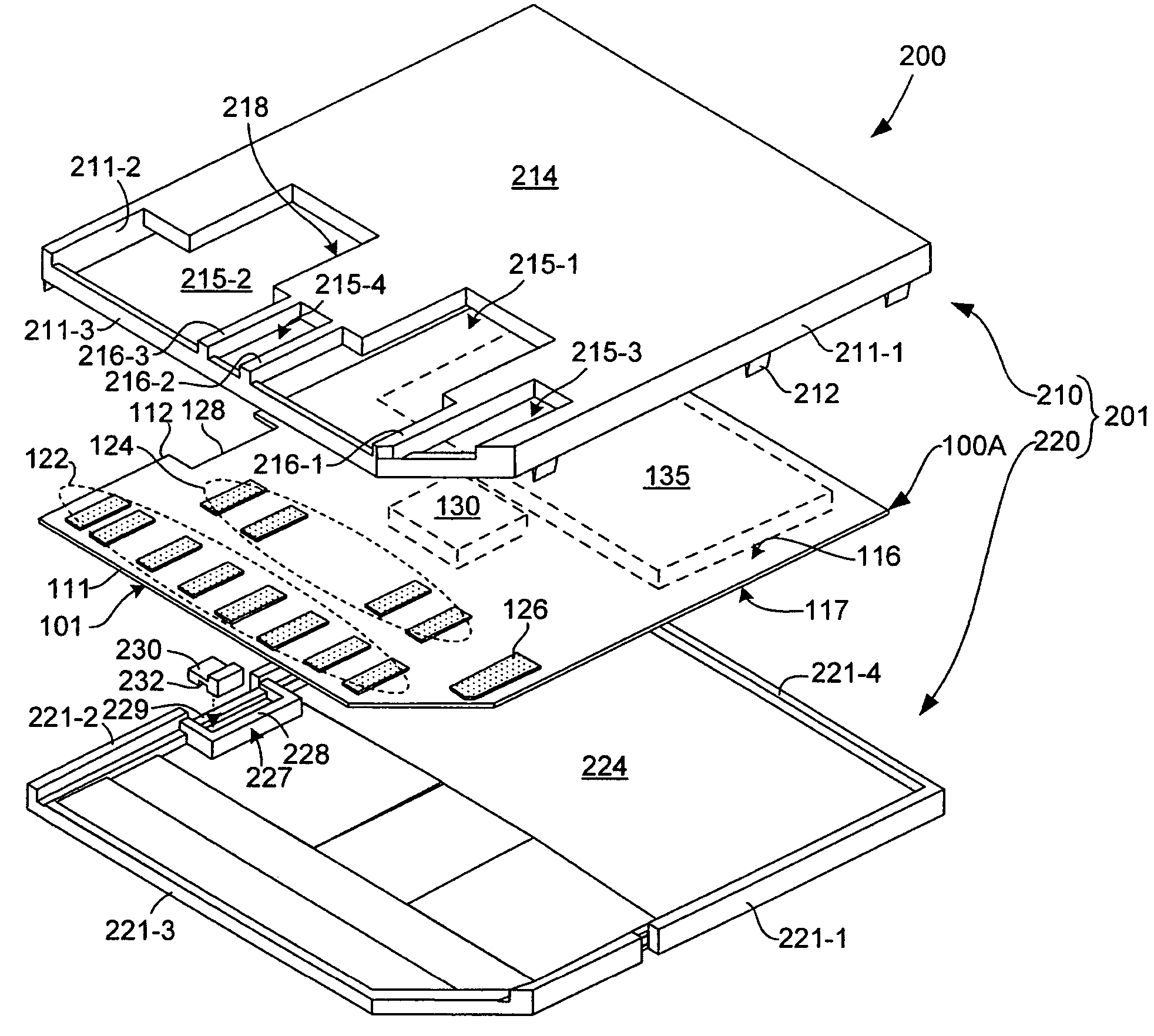
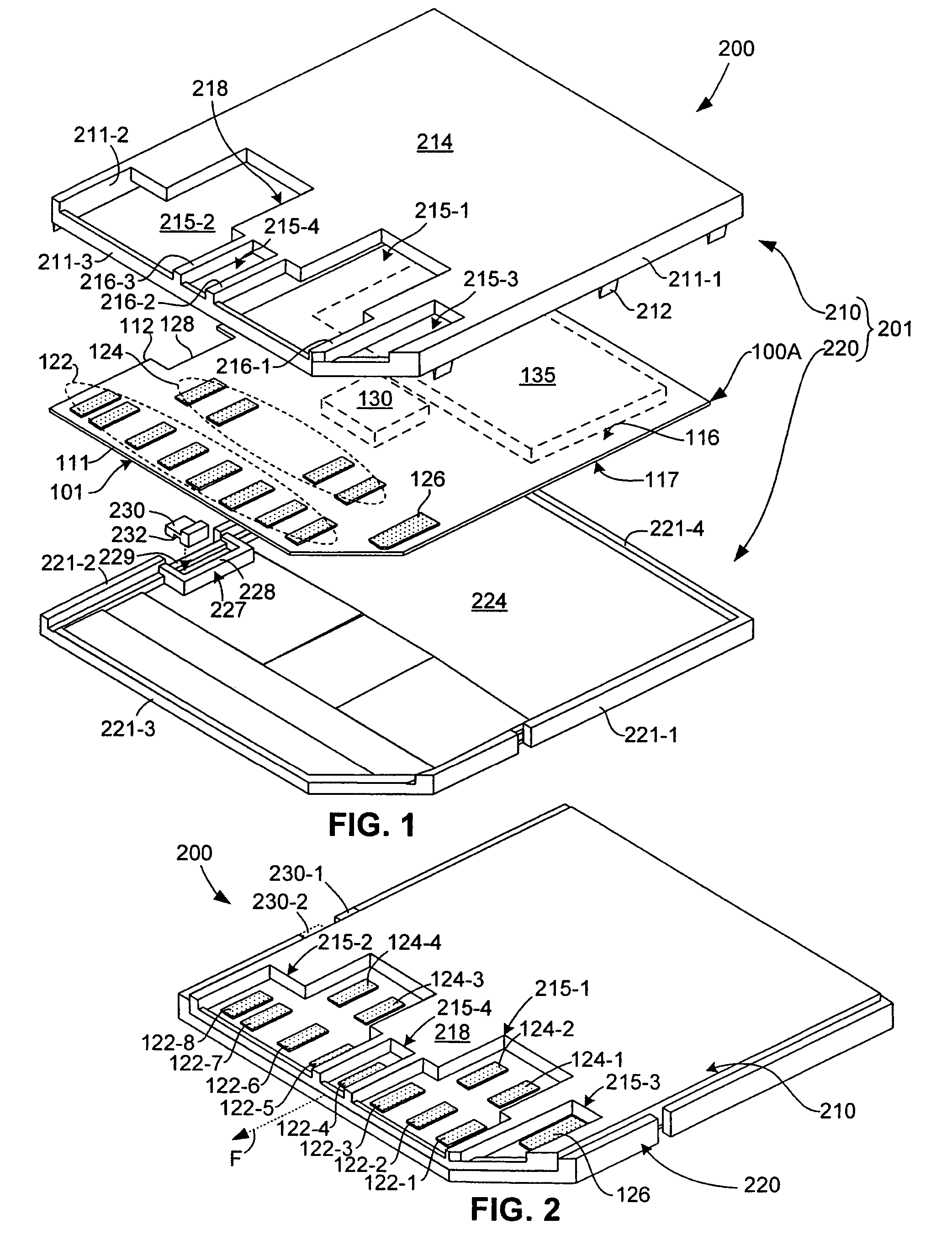
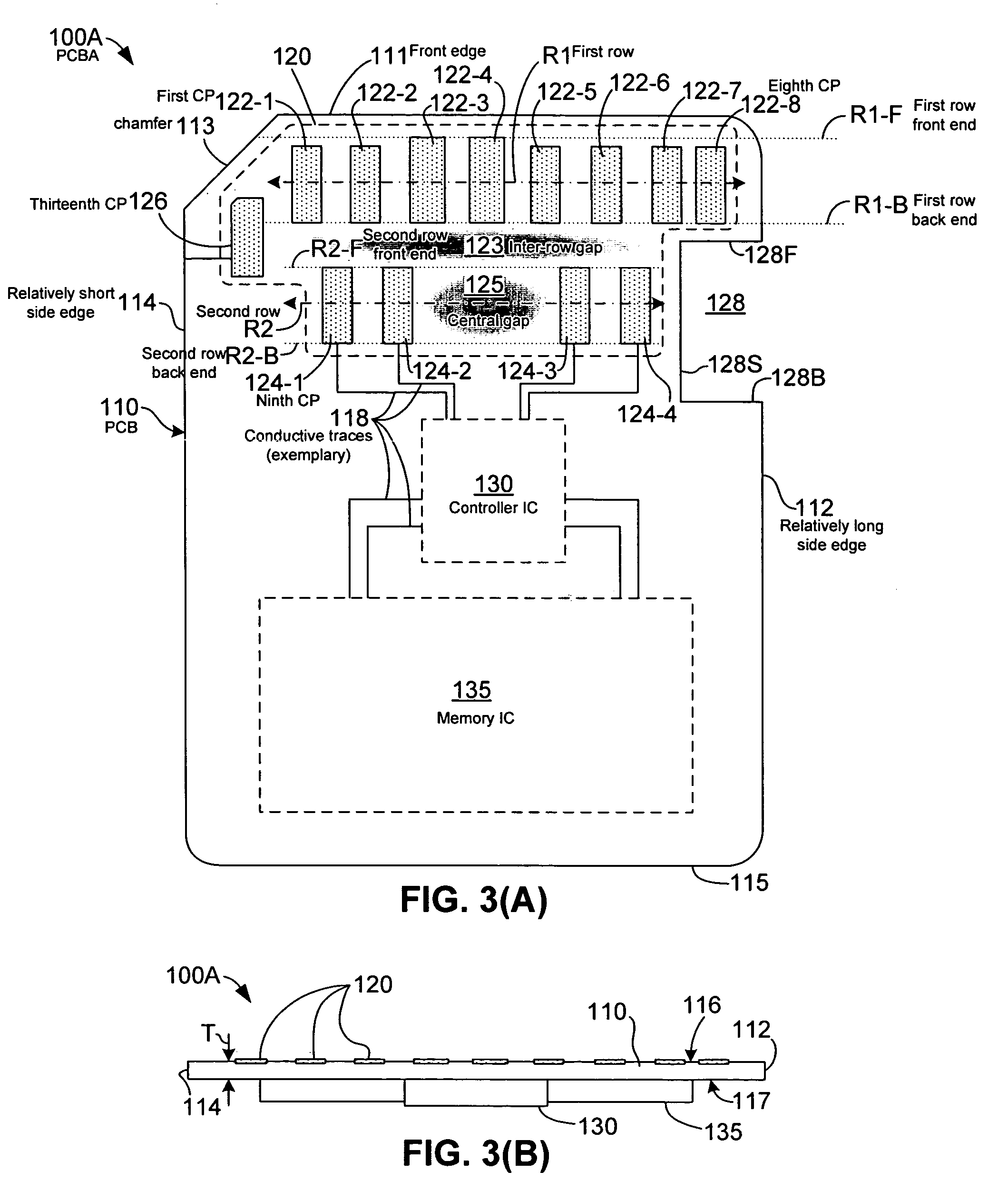
[0025]FIGS. 1 and 2 are exploded perspective and assembled perspective views, respectively, showing a 13-pad memory card 200 according to an exemplary embodiment of the present invention. Memory card 200 generally includes a printed circuit board assembly (PCBA) 100A and a two-part housing 201 including an upper cover 210 and a lower cover 220 that are mounted over PCBA 100A in the manner shown in FIG. 2.

[0026]According to an aspect of the present invention, PCBA 100A is constructed in a manner that is consistent with MMC Specification Version 4.0 mechanical form factors, which were announced by MultiMediaCard (MMC) Association (www.mmca.org) in February 2004, and housing 201 is constructed in a manner that is consistent with mechanical form factors established by SD Card Association (www.sdcard.org). In particular, PCBA 100A includes thirteen contact pads arranged in a pattern consistent with MMC Specification Version 4.0, and housing 201 is formed with dimensions that comply with ...


PUM


Abstract

A memory card including a PCB assembly that is consistent with existing 13-pad MMC mechanical form factors, and a housing that is consistent with the SD mechanical form factor, thereby providing a single PCBA and housing arrangement that can be used to produce both MMC and SD memory cards. The thirteen contact pads support all MMC and SD contact pad patterns, but are modified to facilitate a write protect switch. The housing includes an enlarged window (or windows) that exposes two or more contact pads in each of the multiple rows, thereby facilitating slidable insertion of the memory card into a socket of a host system. Alignment notches are formed in the side edges of the PCB, and / or alignment pins are utilized for properly aligning the PCBA within the housing.

Description

BACKGROUND OF THE INVENTION[0001]1. Field of the Invention[0002]This invention relates to removable memory cards, and more particularly to removable memory cards for dual-protocol systems.[0003]2. Related Art[0004]Flash-memory cards are widely used for storing digital pictures captured by digital cameras. One useful format is the Secure-Digital (SD) format, which is an extension of the earlier MultiMediaCard (MMC) format. Such memory cards are also useful as add-on memory cards for other devices, such as portable music players, personal digital assistants (PDAs), and even notebook computers. SD cards are hot-swappable, allowing the user to easily insert and remove SD cards without rebooting or cycling power. Since the SD cards are small, durable, and removable, data files can easily be transported among electronic devices by being copied to an SD card. SD cards are not limited to flash-memory cards, but other applications such as communications transceivers can be implemented as SD ...

Claims


Application Information

Patent Timeline
Patent Type & Authority Patents(United States)
IPC IPC(8): G06K19/06G06K19/077H05K1/11
CPCG06K19/077G06K19/07732H05K1/117H05K1/0295H05K2201/09954H05K2201/094H05K2201/09409
Inventor WANG, KUANG-YUNI, JIMSEE, SUN-TECK
Owner SUPER TALENT ELECTRONICS
Why Eureka
Try Eureka