Electronic component mounting apparatus and electronic component mounting method

a technology for mounting apparatuses and electronic components, applied in metal working apparatuses, manufacturing tools, soldering apparatuses, etc., can solve the problems of reducing the weight of the mounting head, the degree to which the structure of the mounting head can be simplified, and the increase in the speed of the mounting operation is precluded, and the substrate is delayed

Inactive Publication Date: 2006-04-25
PANASONIC CORP
View PDF15 Cites 161 Cited by
  • Summary
  • Abstract
  • Description
  • Claims
  • Application Information

AI Technical Summary

Benefits of technology

[0043]According to the present invention, since the electronic component acquired from the electronic component feeding unit is placed on the viscous liquid that is spread out on a flat stage, the coating of the bumps with the viscous liquid is completed, and the electroni

Problems solved by technology

Therefore, since the strength of the mounting head must be increased to withstand the strain imposed by the application of pressure, the degree to which the structure of the mounting head can be simplified, and its weight reduced, is limited, an

Method used


Image

  • Electronic component mounting apparatus and electronic component mounting method
  • Electronic component mounting apparatus and electronic component mounting method
  • Electronic component mounting apparatus and electronic component mounting method

Examples


first embodiment

(First Embodiment)

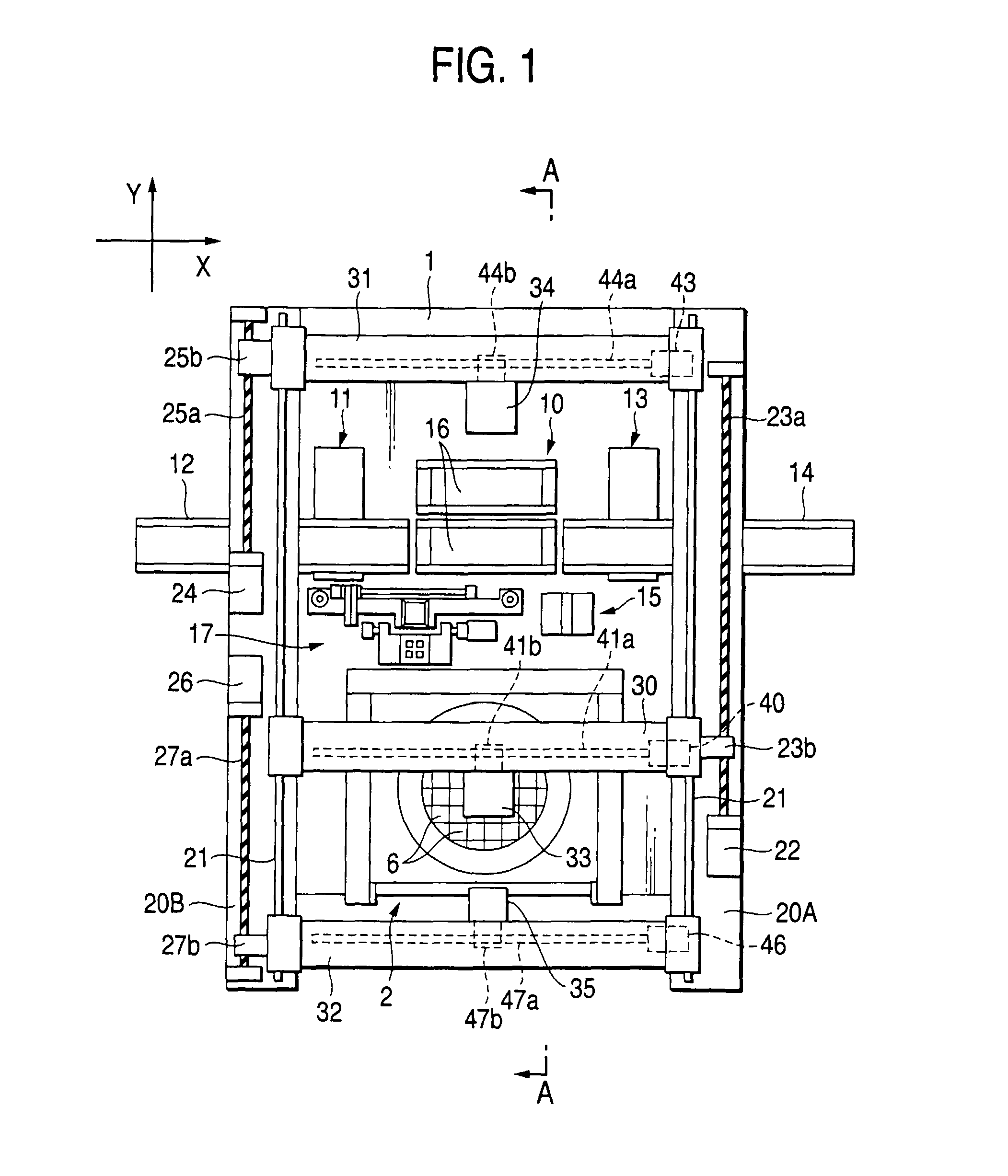
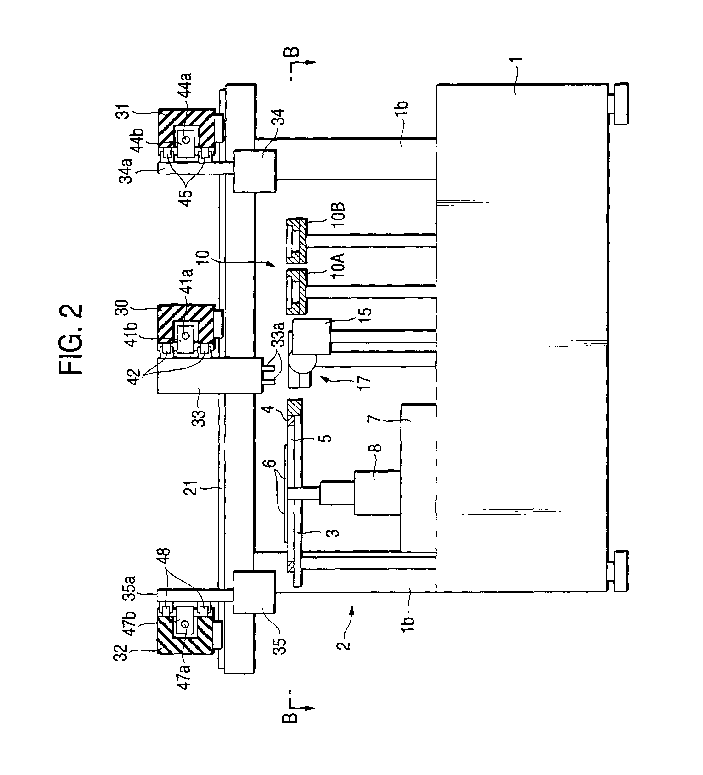
[0071]FIG. 1 is a plan view of an electronic component mounting apparatus according to a first embodiment of the present invention. FIG. 2 is a side, cross-sectional view of the electronic component mounting apparatus according to the first embodiment. FIG. 3 is a plan, cross-sectional view of the electronic component mounting apparatus according to the first embodiment. FIG. 4 is a perspective view of the inversion unit of the electronic component mounting apparatus according to the first embodiment. FIGS. 5A, 5B and 6A to 6E are diagrams for explaining the movement of components during the inversion unit of the electronic component mounting apparatus according to the first embodiment. FIG. 7 is a block diagram showing the configuration of the control system of the electronic component mounting apparatus according to the first embodiment. FIG. 8 is a functional block diagram showing the functions performed by the electronic component mounting apparatus according t...

second embodiment

(Second Embodiment)

[0156]FIG. 15 is a plan view of an electronic component mounting apparatus according to a second embodiment of the invention. FIG. 16 is a side cross-sectional view of the electronic component mounting apparatus according to the second embodiment of the invention. FIG. 17 is a plan cross-sectional view of the electronic component mounting apparatus according to the second embodiment of the invention. FIG. 18 is a block diagram showing the configuration of the control system of the electronic component mounting apparatus according to the second embodiment of the invention. FIG. 19 is a functional block diagram showing the process functions of the electronic component mounting apparatus according to the second embodiment of the invention. FIG. 20 is a timing chart showing the electronic component mounting method according to the second embodiment of the invention. And FIGS. 21A to 21B, 22A to 22B, 23A to 23B, and 24A to 24B are diagrams for explaining procedural ste...

third embodiment

(Third Embodiment)

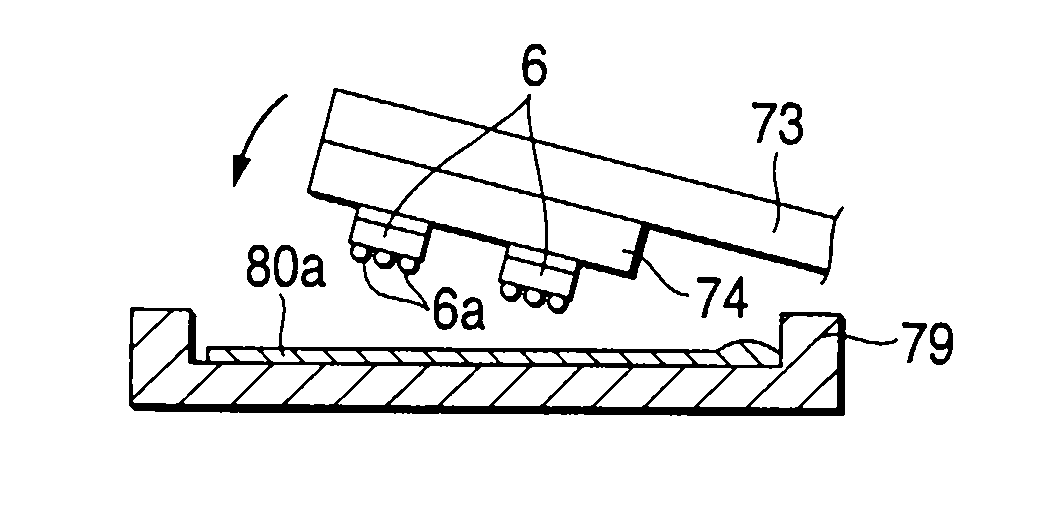
[0182]FIG. 25 is a plan cross-sectional view of an electronic component mounting apparatus according to a third embodiment of the present invention, and FIGS. 26A and 26B are diagrams for explaining the procedural steps for an electronic component mounting method according to the third embodiment. In the third embodiment, for the electronic component mounting apparatus in the second embodiment, the electronic component feeding unit 2 for supplying the chips 6 attached to the adhesive sheet 5 is replaced with a unit for supplying chips that are retained in a tray in the face-down state, wherein the bump formation face is directed downward.

[0183]In the plan view in FIG. 25 for the electronic component mounting apparatus, an inversion unit 17, a third camera 15, a substrate holder 10, a substrate sorter 11 and a substrate relay unit 13, all of which have the same structures as those in the first embodiment, are provided on a base anvil 1, and an electronic component f...


PUM

PropertyMeasurementUnit
Timeaaaaaaaaaa
Viscosityaaaaaaaaaa

Abstract

The present invention provides an electronic component mounting apparatus, wherein a high speed operation can be provided by simplifying the structure of a mounting head and wherein the working efficiency can be improved by eliminating the use of the mounting head for a coating process. In the electronic component mounting apparatus, a flux is coated on chips supplied to an electronic component feeding unit while bump formation faces are directed upward. The chips are mounted on a substrate. A holding head receives the chips extracted from an adhesive sheet by a mounting head and is inverted relative to a stage on which a flux is spread. As a result, the bumps of the chips are covered with the flux and are flattened, and after the holding head is returned to the original stage, the chips on the stage are extracted and mounted on the substrate by the mounting head.

Description

BACKGROUND OF THE INVENTION[0001]1. Field of the Invention[0002]The present invention relates to an electronic component mounting apparatus for mounting electronic components on a substrate, and to an electronic component mounting method.[0003]2. Description of the Related Art[0004]When in use, an electronic component mounting apparatus repetitively performs a mounting operation, wherefor a mounting head is employed, to securely mount on a substrate electronic components supplied by an electronic component feeding unit. Of the electronic components thus supplied, an electronic component such as a flip chip, on the surface of which are formed bumps, projecting electrodes used for connections, is generally fed with the bump formation surface facing upward.[0005]Such an electronic component is extracted from the electronic component feeding unit by a special pickup device, for which an inversion mechanism is provided, and is inverted and is held with the bumps directed downwards. The m...

Claims


Application Information

Patent Timeline
IPC IPC(8): H01L21/60H01L21/67H01L21/00H01L21/68
CPCH01L21/67144H01L21/6715H01L21/681Y10T29/53178Y10T29/53183Y10T29/53191H01L24/75H05K13/04
Inventor HAJI, HIROSHIHIRAKAWA, TOSHIRO
Owner PANASONIC CORP
Why Eureka
Try Eureka