Luminescent Light Source, Method for Manufacturing the Same, and Light-Emitting Apparatus

a technology of light-emitting elements and light-emitting tubes, which is applied in the manufacture of electric discharge tubes/lamps, luminescent screens, lighting and heating apparatus, etc. it can solve the problems of uneven chromaticity of output light, a gap is likely to form between the underfill and the phosphor layer, and the underfill is likely to be peeling at the interface therein, so as to reduce the cycle time and prevent peeling. , the effect of uniform thickness o

Inactive Publication Date: 2007-10-04
PANASONIC CORP
View PDF0 Cites 42 Cited by
  • Summary
  • Abstract
  • Description
  • Claims
  • Application Information

AI Technical Summary

Benefits of technology

[0015] According to the present invention, even without the use of an underfill, a gap between a light-emitting element and a substrate can be eliminated. Thus, a luminescent light source that prevents the deformation of a phosphor layer and the formation of a through-hole resulting from air leakage so as to achieve a uniform thickness of the phosphor layer, and a light-emitting apparatus using the same can be provided.
[0016] Furthermore, according to the present invention, since an underfill is not used, it is possible to reduce cycle time by eliminating the process of filling an underfill from the conventional processes and prevent peeling that occurs at an interface between an underfill and a phosphor layer. Thus, a practical method for manufacturing the luminescent light source according to the present invention can be provided.

Problems solved by technology

Such a case causes a phosphor layer to have an unstable shape, that is, the phosphor layer covering the LED bare chip to have a non-uniform thickness, leading to uneven chromaticity of output light, which is problematic.
Moreover, in the case where an underfill and a phosphor layer are formed of different materials from each other, particularly, when the phosphor layer contains a silicone resin having less adhesiveness, peeling is likely to occur at an interface between the underfill and the phosphor layer, which also is problematic.
Because of this, without the use of an underfill, in a conventional method, a material constituting a phosphor layer hardly flows into between a LED bare chip and a substrate, resulting in the formation of a gap therein.
This case causes the phosphor layer covering the LED bare chip to have a non-uniform thickness, leading to, for example, uneven chromaticity of output light and a decrease in luminous efficiency, which are problematic.
Furthermore, when a gap exists between a LED bare chip and a substrate, water is accumulated to cause ion migration across electrodes of the substrate and across p-n junctions of the LED bare chip as well as deterioration of the LED bare chip.

Method used


Image

  • Luminescent Light Source, Method for Manufacturing the Same, and Light-Emitting Apparatus
  • Luminescent Light Source, Method for Manufacturing the Same, and Light-Emitting Apparatus
  • Luminescent Light Source, Method for Manufacturing the Same, and Light-Emitting Apparatus

Examples


example

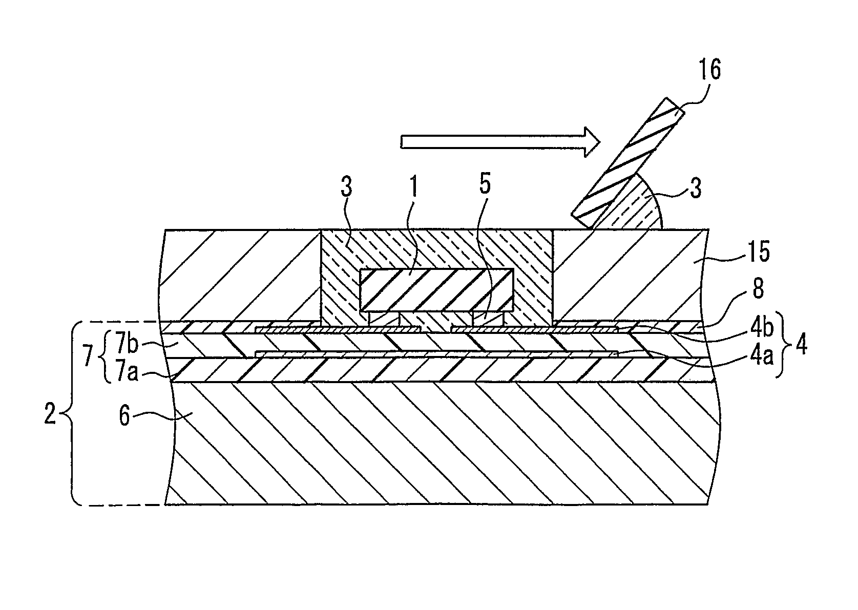
[0096] In this example, as a light-emitting apparatus, a card type light emitting apparatus that has the same configuration as that of the light-emitting apparatus shown in FIGS. 12 and 13 and includes 64 LED bare chips was produced. Further, the light-emitting apparatus according to this example is configured by using a plurality of luminescent light sources of the same configuration as that of the luminescent light source shown in FIG. 5. Accordingly, reference can be made to FIG. 5 as a partial cross-sectional view for this example and to FIGS. 1 to 4 as partial cross-sectional views showing a manufacturing method according to this embodiment.

[0097] Initially, a substrate 2 was produced in the following manner. First, an epoxy resin containing an inorganic filler and copper foil (thickness: 10 μm) were laminated on a metal base 6 formed of an aluminum plate (size: 3 cm by 3 cm, thickness: 1 mm) and subjected to thermocompression to form an insulating layer 7a (thickness: 100 μm)...


PUM


Abstract

A luminescent light source includes: a light-emitting element (1); a substrate (2) including a conductor pattern (4); and a phosphor layer material (3) containing a phosphor and a light-transmitting base material. In the luminescent light source, the light-emitting element (1) is connected to a conductor pattern (4b), and the phosphor layer material (3) covers the light-emitting element (1). Further, at least the light-transmitting base material in the phosphor layer material (3) is disposed between the light-emitting element (1) and the substrate (2). Thus, a luminescent light source can be provided that allows a gap between a light-emitting element such as a LED bare chip or the like and a substrate to be eliminated, thereby obtaining output light with even chromaticity and achieving high luminous efficiency.

Description

TECHNICAL FIELD [0001] The present invention relates to a luminescent light source using a light-emitting element, specifically, a light-emitting diode bare chip, a method for manufacturing the same, and a light-emitting apparatus using the luminescent light source. BACKGROUND ART [0002] In recent years, a luminescent light source using a light-emitting diode bare chip (hereinafter, referred to as a LED bare chip) has been attracting attention as a next-generation illumination light source. The reason behind this is that a luminescent light source using a LED bare chip has longer life and uses no Hg so as to be environmentally friendly compared with conventional incandescent lamps and fluorescent lamps. Another reason is that a LED bare chip itself is small and thus allows a luminescent light source to be reduced in size and weight. [0003] Examples of a luminescent light source using a LED bare chip include a luminescent light source that includes a LED bare chip, a substrate connec...

Claims


Application Information

Patent Timeline
Patent Type & Authority Applications(United States)
IPC IPC(8): H01J1/62H01J9/00H01L33/50H01L33/56H01L33/60H01L33/62
CPCF21K9/00H01L33/505H01L33/54H01L2224/16H01L2924/0102F21Y2105/001H01L2924/01079H01L2924/09701H01L2924/01322H01L2924/12041H01L2924/01063F21Y2105/10F21Y2115/10H01L2924/00014F21S6/003H01L2924/00011H01L2224/0401
Inventor TANIMOTO, NORIYASUYANO, TADASHITAKAHASHI, KIYOSHISHIMIZU, MASANORIOGATA, TOSHIFUMI
Owner PANASONIC CORP
Why Eureka
Try Eureka