Surface-emitting laser diode with tunnel junction and fabrication method

a laser diode and laser diode technology, applied in semiconductor lasers, laser details, electrical equipment, etc., can solve the problems of difficult downsizing, consumer products are still small, and the production volume of optical fibers is still small, and achieve high repeatability in mass production, eliminate complex processes, and excellent characteristics

Inactive Publication Date: 2006-12-21
FUJIFILM BUSINESS INNOVATION CORP
View PDF7 Cites 41 Cited by
  • Summary
  • Abstract
  • Description
  • Claims
  • Application Information

AI Technical Summary

Benefits of technology

[0027] The present invention has been made in view of the above circumstances and provides a long-wavelength VCSEL with excellent characteristics and high repeatability in mass production and the fabrication method thereof that eliminates complex processes.

Problems solved by technology

This demands temperature control of the device and causes a problem that downsizing is difficult.
In addition, the production volume of the optical fibers is still small, as compared to the consumer products, largely because telecommunications carriers are the users of the optical fibers.
Therefore, the laser diodes are considered costly devices.
The high price is also disturbs in spreading.
In fact, VCSELs in the long-wavelength range have more problems than those in the short-wavelength range.
Therefore, it is still impossible to replace the edge-emitting laser diodes.
The film having a large number of periods increases the device resistance value and degrades the heat dissipation capacity.
It is not desirable in view of the reliability.
That is to say, it is considered difficult to fabricate the reflector almost completely reflective, namely, 99 percent at least, by epitaxially growing the InP substrate lattice matched, in the long-wavelength VCSEL having the InGaAsP-based material.
In most cases, this results in the nonradiative recombination that the carriers are changed to thermal outputs.
It is to be noted that the structure having GaInNAs-based material, even if the material used for the quantum well active layer and the thickness thereof are controlled as much as possible, there is the problem in that it is difficult to increase the oscillation wavelength up to 1.31 μm, namely, zero dispersion of optical fiber, without sacrificing the reliability or electric or optical characteristics.
Light absorption increases as the carrier concentration is increased in the p-type DBR layer, causing degradation in the luminous efficiency.
There are drawbacks for practical use.
Nevertheless, the increase in temperature cannot be avoided when the impurity region or the periphery thereof are processed in the etch, oxidation, and crystal regrowth so as to form the current funneling region.
This makes it difficult to provide the oxidized region with repeatability.
On the VCSEL, the current funneling region plays an important role in deciding the characteristics of the whole device, yet the low repeatability in process causes the variations in the diameter of the opening provided in the current funneling region.
As a result, the characteristics vary depending on the process lot, which might degrade the mass productivity.
However, Japanese Laid-Open Patent Publication No. 2004-247728 does not describe in detail how the current funneling region is created.
The current may not be confined especially, as so-called simple pillar structure, yet ineffective recombination will be increased and the luminous efficiency will not be enhanced.
As described, there has not been available the long-wavelength VCSEL that exhibits sufficient characteristics in view of the structure.

Method used


Image

  • Surface-emitting laser diode with tunnel junction and fabrication method
  • Surface-emitting laser diode with tunnel junction and fabrication method
  • Surface-emitting laser diode with tunnel junction and fabrication method

Examples


embodiments

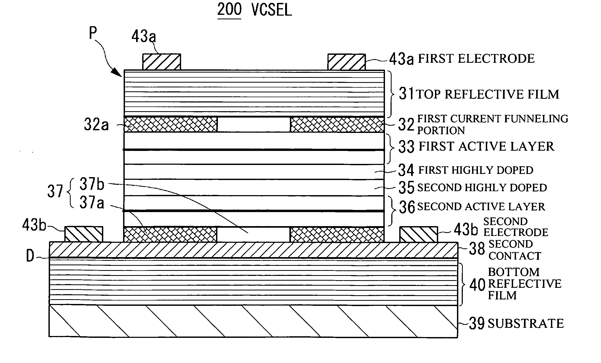
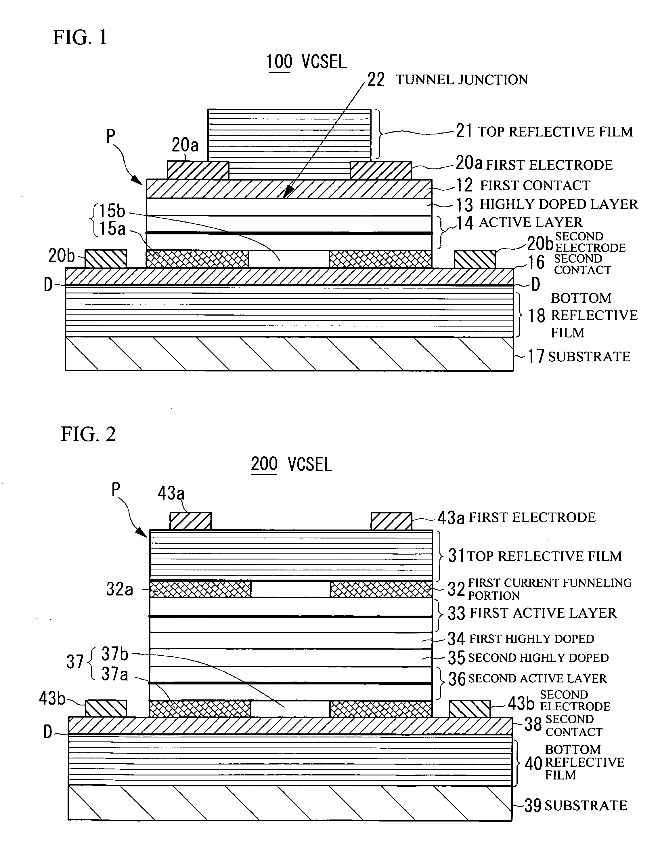
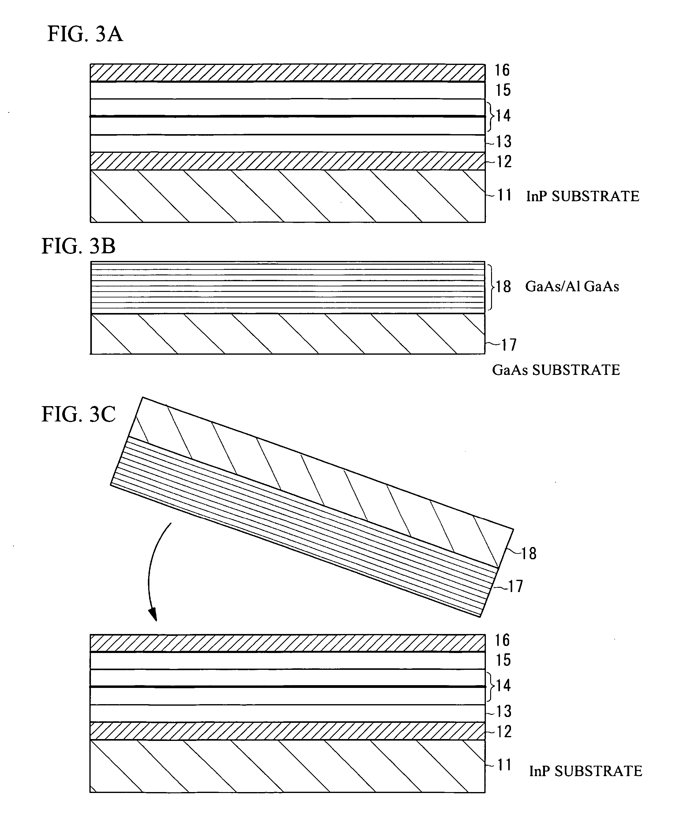
[0048]FIG. 1 is a cross-sectional view of a VCSEL in accordance with a first embodiment of the present invention. Referring to FIG. 1, a VCSEL 100 in accordance with the first embodiment of the present invention includes an undoped semiconductor substrate 17. On the semiconductor substrate 17, there are successively provided from the bottom, an undoped bottom reflective film 18 composed of semiconductor multiple films of GaAs / AlGaAs, an n-type second contact layer 16, an n-type current funneling layer 15 that includes a layer having high concentration of aluminum, an active region 14 composed of undoped spacer layers and a quantum well active layer disposed therebetween, a highly doped layer 13 with p-type high impurity concentration, a first contact layer 12 with n-type high impurity concentration, and a top reflective film 21 composed of dielectric multiple films of TiO2 / SiO2. The top and bottom reflective films 18 and 21 serve as DBRs (Distributed Bragg Reflectors). The current f...


PUM


Abstract

A surface emitting semiconductor laser diode includes a semiconductor substrate, a first reflective film provided on the semiconductor substrate, a second reflective film provided above the first reflective film, an active region, a tunnel junction region, and a current funneling layer. The active region, the tunnel junction region, and the current funneling layer are provided in series between the first and second reflective films, the active region being interposed by the tunnel junction region and the current funneling layer.

Description

BACKGROUND OF THE INVENTION [0001] 1. Field of the Invention [0002] This invention relates to surface-emitting laser diodes with tunnel junctions and fabrication methods thereof, which are used for light sources of optical information processing or high-speed optical communication. [0003] 2. Description of the Related Art [0004] In recent years, attention has been attracted to surface emitting laser diodes, in particular, to Vertical-Cavity Surface-Emitting Laser diodes (hereinafter, referred to as VCSEL) in the technical fields of the optical communication and optical storage. [0005] VCSEL has excellent characteristics that are not provided by conventional edge-emitting laser diodes. For example, VCSEL have low threshold current and low power consumption. An optical spot is easily obtainable. The device can be tested at the wafer level. The structure can be integrated in a two-dimensional array configuration. Expectations for VCSEL having the afore-mentioned advantages are raised a...

Claims


Application Information

Patent Timeline
Patent Type & Authority Applications(United States)
IPC IPC(8): H01S5/00
CPCB82Y20/00H01S2302/00H01S5/0217H01S5/02284H01S5/02288H01S5/0421H01S5/18311H01S5/18325H01S5/1833H01S5/18341H01S5/18369H01S5/18383H01S5/18397H01S5/3095H01S5/34306H01S5/3434H01S5/0215H01S5/02251H01S5/02253
Inventor UEKI, NOBUAKI
Owner FUJIFILM BUSINESS INNOVATION CORP
Why Eureka
Try Eureka