Reflective and transmissive mode monolithic millimeter wave array system and in-line amplifier using same

a millimeter wave array and transmittance mode technology, applied in the field of mirror-on-ductor power devices, can solve the problems of high cost of sources, devices that implement these technologies (tubes) may cost millions of dollars each, and the cost of sources is very high

Inactive Publication Date: 2006-04-25
RAYTHEON CO
View PDF11 Cites 14 Cited by
  • Summary
  • Abstract
  • Description
  • Claims
  • Application Information

AI Technical Summary

Problems solved by technology

However, these sources are very expensive.
However these devices range from $10,000 to $20,000 in cost.
However, devices implemented with these technologies (tubes) may cost millions of dollars each.
In general, devices implemented with conventional technologies do not generate affordable power in the W-band.
In addition, the flexibility of conventional power systems, such as Gunn and Impatt diodes and InP HEMT amplifiers, is limited.

Method used


Image

  • Reflective and transmissive mode monolithic millimeter wave array system and in-line amplifier using same
  • Reflective and transmissive mode monolithic millimeter wave array system and in-line amplifier using same
  • Reflective and transmissive mode monolithic millimeter wave array system and in-line amplifier using same

Examples


Embodiment Construction

[0027]While the present invention is described herein with reference to illustrative embodiments for particular applications, it should be understood that the invention is not limited thereto. Those having ordinary skill in the art and access to the teachings provided herein will recognize additional modifications, applications, and embodiments within the scope thereof and additional fields in which the present invention would be of significant utility.

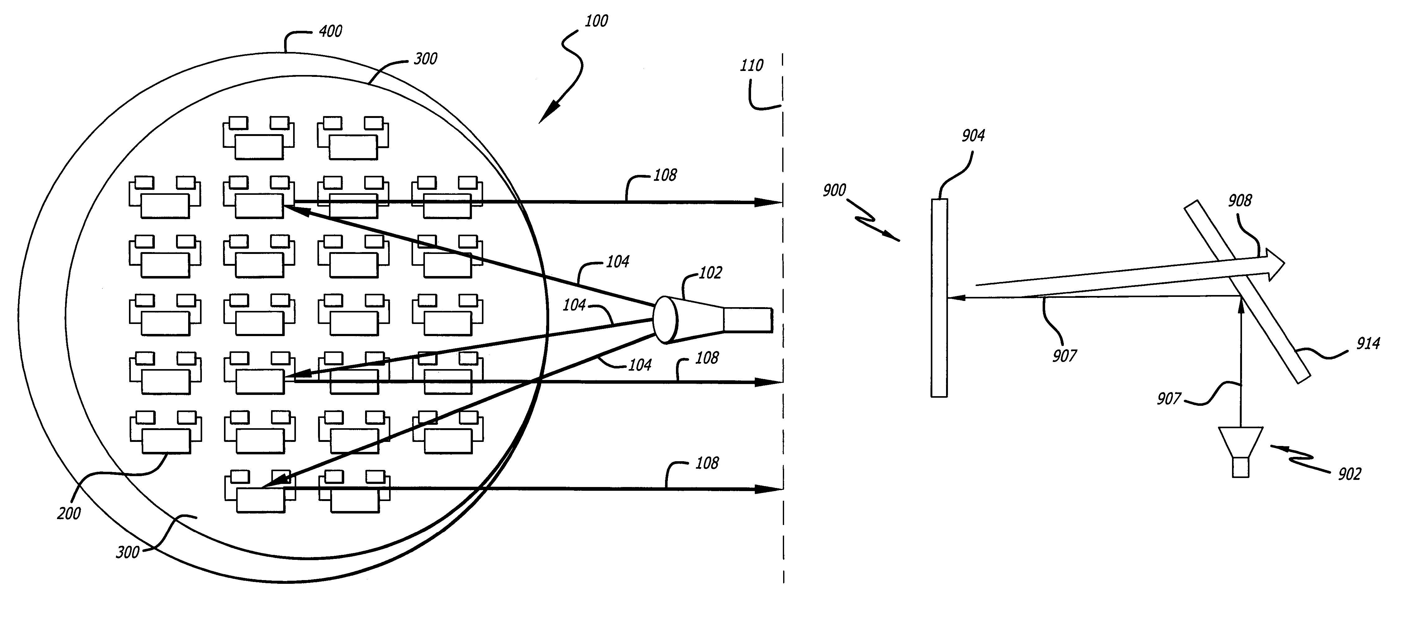
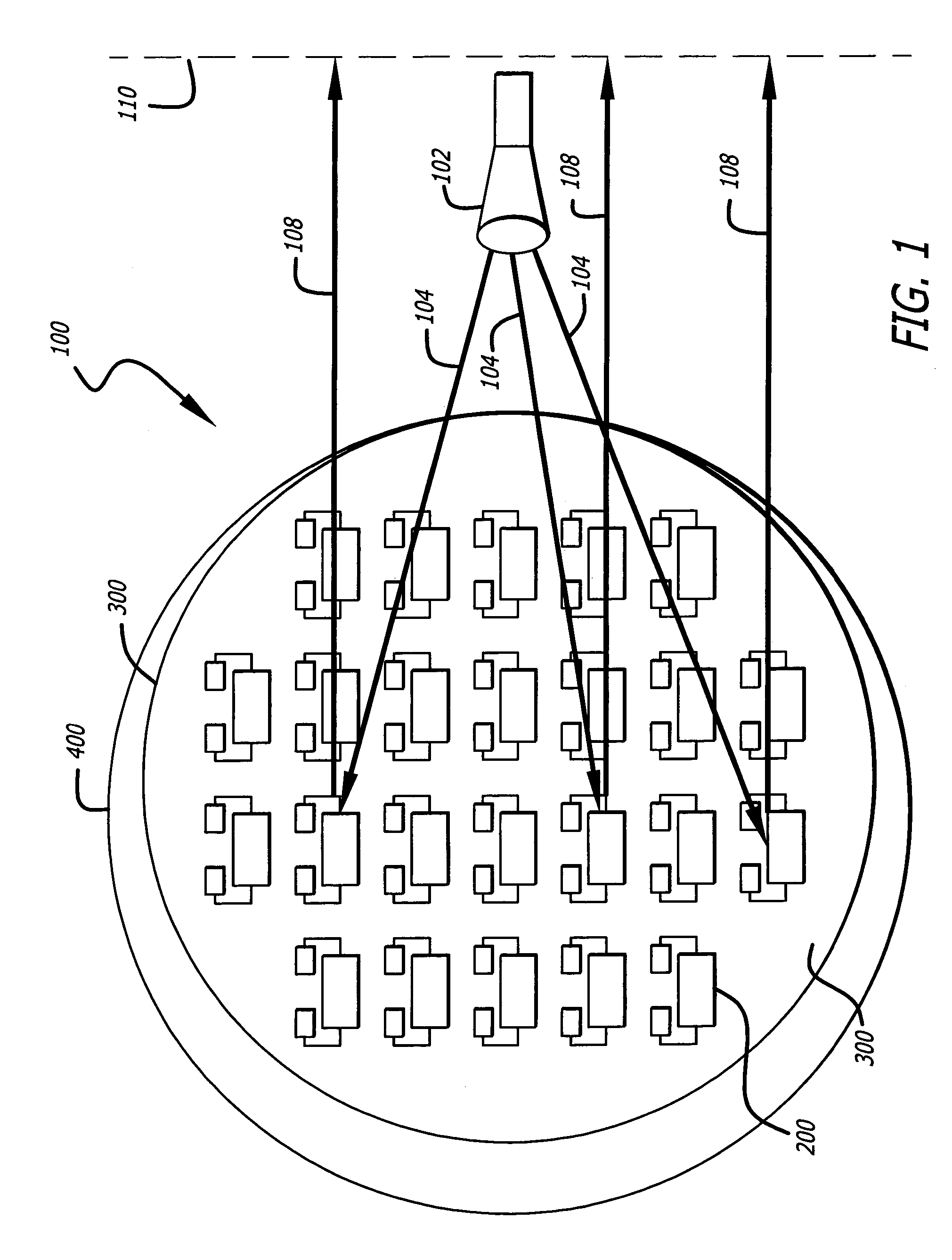
[0028]The present invention is designed to produce high energy density and high power level RF / Millimeter wave radiation using the quasi-optical spatial power of an array of small amplifiers on a solid state wafer. In an illustrative reflective mode implementation, each cell of the array contains a reflection amplifier that receives radiation and retransmits the amplified signal back into the approximate same direction from which it was received. The radiation exiting from the array is physically like a reflection that has been modifi...


PUM


Abstract

An amplifier including a monolithic semiconductor substrate and an array disposed on said substrate for coherently receiving and retransmitting electromagnetic energy. The array is implemented with a plurality of cells. Each of the cells includes a dual polarization antenna structure for receiving electromagnetic energy and an amplifier connected thereto. The amplifier may include an ortho-mode feed and a reflective amplifier array adapted to be illuminated by the feed with an input wavefront with a first polarization and to return thereto an amplified wavefront with a second polarization orthogonal to the first wavefront. First and second shaped mirrors may be incorporated for illuminating the array with a planar wavefront and converting the reflected planar wavefront to a spherical wavefront.

Description

REFERENCE TO RELATED APPLICATION[0001]This is a continuation in part of U.S. patent application Ser. No. 10 / 153,140 filed May 20, 2002 by K. W. Brown et al. now U.S. Pat. No. 6,765,535 and entitled MONOLITHIC MILLIMETER WAVE REFLECTOR ARRAY SYSTEM the teachings of which are hereby incorporated herein by reference and from which priority is hereby claimed.BACKGROUND OF THE INVENTION[0002]1. Field of the Invention[0003]This invention relates to power devices. Specifically, the present invention relates to semiconductor power devices.[0004]2. Description of the Related Art[0005]Techniques have been developed for producing W-band semiconductor power devices (e.g. 50 Ghz to 120 Ghz). For example Gunn and Impatt diode sources have been developed which produce ¼ watt of power. However, these sources are very expensive. Indium Phosphide High Electron Mobility Transistor (InP HEMT) amplifiers have been developed which produce 1 / 10 watt of power. However these devices range from $10,000 to $2...

Claims


Application Information

Patent Timeline
Patent Type & Authority Patents(United States)
IPC IPC(8): H01Q1/38H01Q3/46H01Q21/00H01Q21/06H01Q23/00
CPCH01Q3/46H01Q21/0018H01Q23/00H01Q21/061H01Q21/065H01Q21/0093
Inventor BROWN, KENNETH W.GALLIVAN, JAMES R.
Owner RAYTHEON CO
Why Eureka
Try Eureka