Semiconductor integrated circuit device

a technology of integrated circuit and semiconductor, applied in the direction of overvoltage protection resistors, emergency protective arrangements for limiting excess voltage/current, arrangements responsive to excess voltage, etc., can solve the problem of parasitic capacity so high as to deteriorate the gain, and it is difficult to apply the protective circuit of the prior art to the circuit of the high-frequency portion, so as to reduce the linearity or the gain deterioration, the effect of parasitic capacity lowering

Inactive Publication Date: 2006-04-25
RENESAS ELECTRONICS CORP
View PDF14 Cites 52 Cited by
  • Summary
  • Abstract
  • Description
  • Claims
  • Application Information

AI Technical Summary

Benefits of technology

[0023]In accordance with the miniaturization of the wireless communication mobile terminal device of recent years, there has been desired and developed a one-chip IC in which the transmission / reception band modulator / demodulator circuits and the high-frequency amplifications are integrated to correspond to the low-noise amplifier 4, the reception mixer 6, the variable-gain controlled amplifier 8, the demodulator 9, the modulator 11, the variable-gain controlled amplifier 12, the transmission mixer 13 and the transmission preamplifier 15, as shown in FIG. 9. It is necessary to protect the entire chip against the high breakdown voltage.

Problems solved by technology

However, it has been found out that the one-chip IC of the prior art incorporating the protective circuit has the following problems.(1) The high-frequency circuit including the low-noise amplifier 4, the reception mixer 6, the transmission mixer 13 and the transmission preamplifier 15 is provided at its input / output circuits with a matching circuit having a capacity and an inductance.
If the circuit having a construction of transistors of one stage is applied as the protective circuit as in the example of the prior art, a bias condition for allowing the electric current to flow through that protective circuit is established to raise a problem that the signal is distorted.(2) On the other hand, the attachment of the protective circuit of the prior art raises a problem that the parasitic capacity is so high as to deteriorate the gain.
This makes it hard to apply the protective circuit of the prior art to the circuit of the high-frequency portion.(3) In the protective circuit having the transistors of a construction of two stages of the prior art, on the other hand, the element structure is constructed of thyristors.
If a high static electricity is applied, therefore, the IC actions cannot be made because an overcurrent continuously flows unless the power supply is broken.

Method used


Image

  • Semiconductor integrated circuit device
  • Semiconductor integrated circuit device
  • Semiconductor integrated circuit device

Examples


embodiment 1

[Embodiment 1]

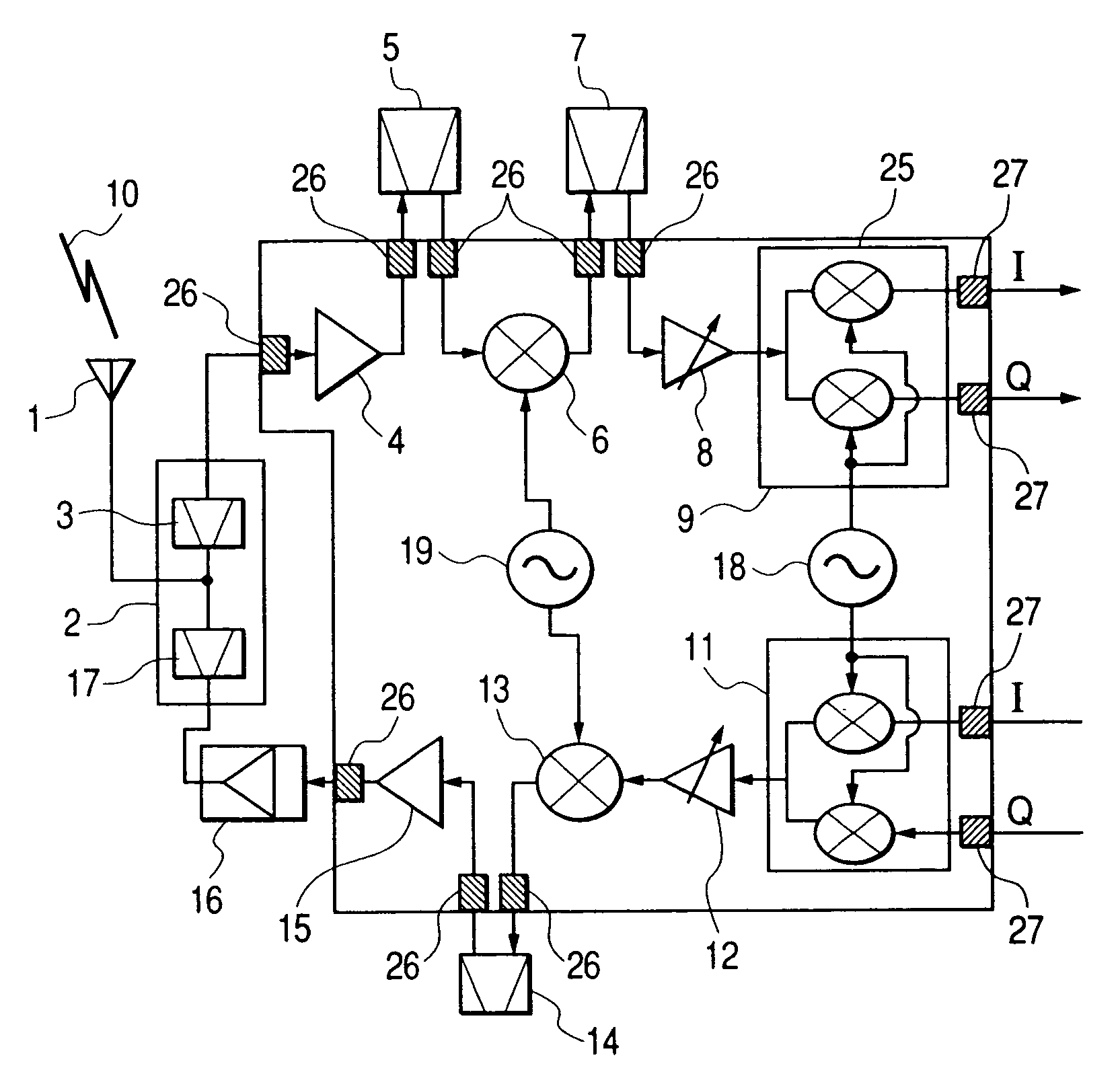
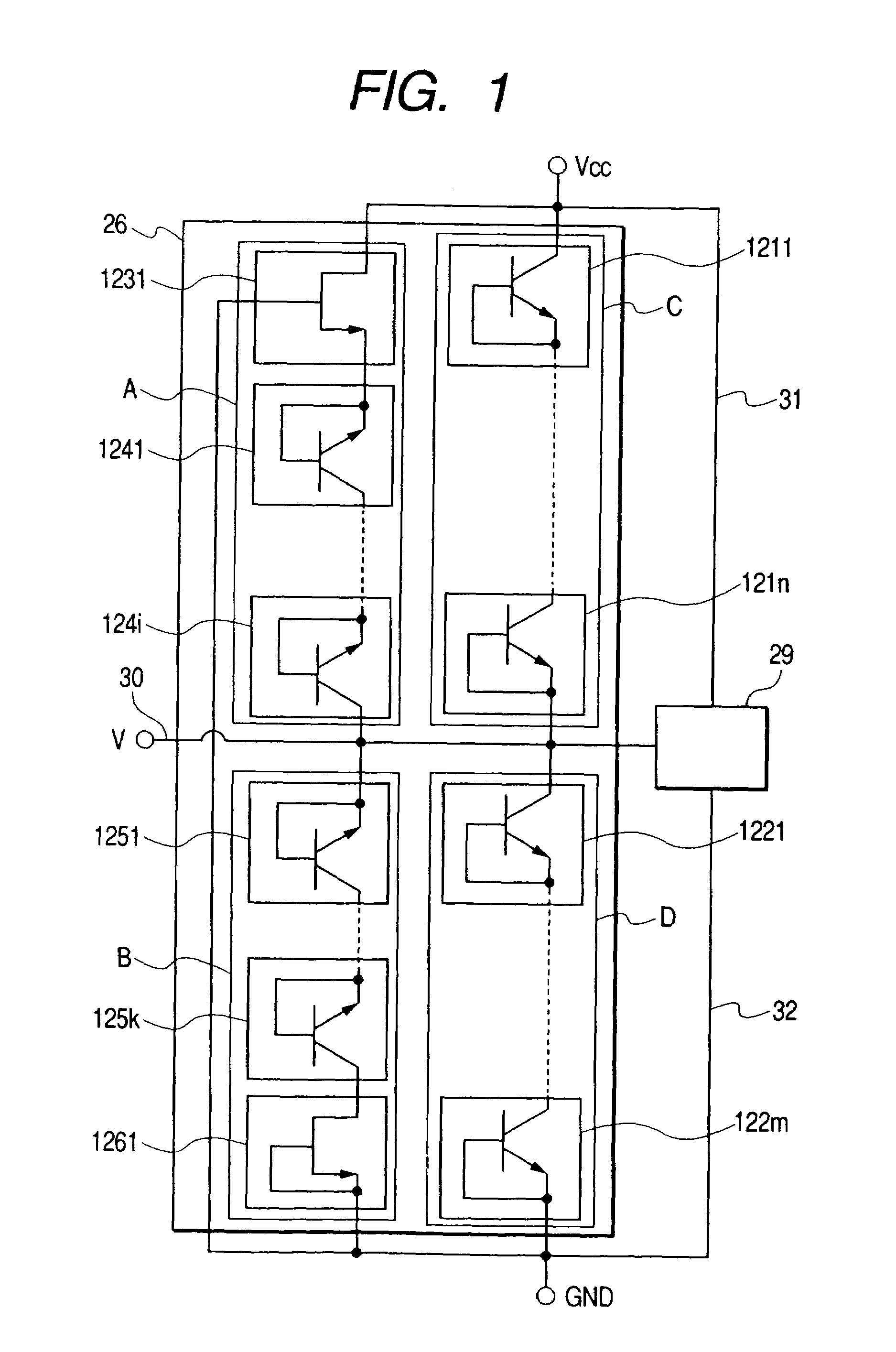
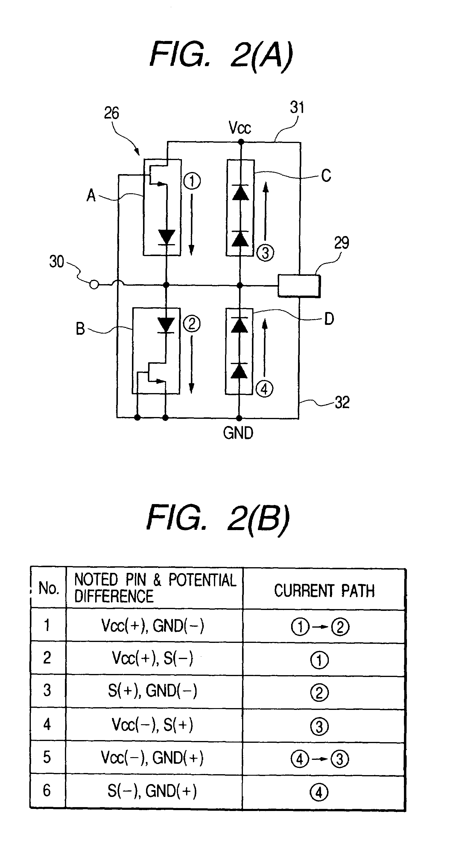
[0066]FIGS. 1 to 7 are diagrams relating to a semiconductor integrated circuit device according to one embodiment (Embodiment 1) of the invention, and FIGS. 1 to 5 are diagrams relating to a protective circuit.

[0067]In Embodiment 1, the invention will be described on the example in which it is applied to a signal processing IC for a cellular phone. Here will be described a construction of the cellular phone. FIG. 5 is a block diagram showing a portion of a system construction of the cellular phone.

[0068]In this block diagram, as in FIG. 9, there are shown a transmission line and a reception line which are connected with an antenna 1 through a duplexer 2. Both of these transmission line and reception line are connected with a not-shown base band.

[0069]The reception line is constructed by connecting the antenna 1, a band-pass filter 3 packaged in the duplexer 2, a low-noise amplifier 4, a band-pass filter 5, a receiving mixer 6, a band-pass filter 7, a variable-gain cont...


PUM


Abstract

Into an internal circuit to operate in a high-frequency band, there is incorporated a protective circuit of a multistage connection which is constructed to include a plurality of diode-connected transistors having a low parasitic capacity and free from a malfunction even when an input signal higher than the power supply voltage is applied. Into an internal circuit to operate in a low-frequency band, there is incorporated a protective circuit which is constructed to include one diode-connected transistor. The protective circuits include two lines of protective circuit, in which the directions of electric currents are so reversed as to protect the internal circuits against positive / negative static electricities.

Description

[0001]This is a continuation application of U.S. Ser. No. 09 / 785,499, filed Feb. 20, 2001, now U.S. Pat. No. 6,665,159.BACKGROUND OF THE INVENTION[0002]The present invention relates to a semiconductor integrated circuit device and, more particularly, to a technique which is effective when applied, in a semiconductor integrated circuit device including circuits for processing signals from an intermediate-frequency band to a high-frequency band, to a protective technique for preventing the electrostatic breakdowns of circuit elements constructing the semiconductor integrated circuit device.[0003]A wireless communication system (or a wireless communication mobile terminal device, as will be shortly called the “terminal device”) such as a digital cellular system has its circuits of transmission line and reception line constructed to include many discrete ICs (semiconductor integrated circuit devices). A representative example of the terminal device, of which the transmission / reception l...

Claims


Application Information

Patent Timeline
Patent Type & Authority Patents(United States)
IPC IPC(8): H01C7/12H01L21/822H01L27/04H01L27/02H03F1/52H04B1/3822H04B1/40
CPCH01L27/0255H03F1/52H01L27/0259H03F2200/372H01L27/04
Inventor TAKIKAWA, KUMIKOTANAKA, SATOSHIKASAHARA, MASUMI
Owner RENESAS ELECTRONICS CORP
Why Eureka
Try Eureka