Method for producing an organic electroluminescence display element

a technology of electroluminescence and display elements, which is applied in the manufacture of electric discharge tubes/lamps, lighting and heating apparatuses, and tube/lamp factory adjustment, etc., and can solve the problem of insufficient effect of improving the luminance lifetime of emission

Inactive Publication Date: 2006-05-09
NIPPON SEIKI CO LTD
View PDF10 Cites 9 Cited by
  • Summary
  • Abstract
  • Description
  • Claims
  • Application Information

AI Technical Summary

Benefits of technology

[0025]In accordance with Embodiment 1 of the present invention, there is provided a method for producing an organic electroluminescence display element having a light emitting layer between an anode and a cathode, which is characterized in that operations are carried out in the combination of aging in a forward direction wherein a

Problems solved by technology

However, even by such treatments, the effect of improvin

Method used


Image

  • Method for producing an organic electroluminescence display element
  • Method for producing an organic electroluminescence display element
  • Method for producing an organic electroluminescence display element

Examples


case 1

[Case 1]

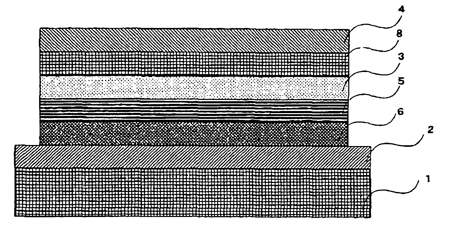
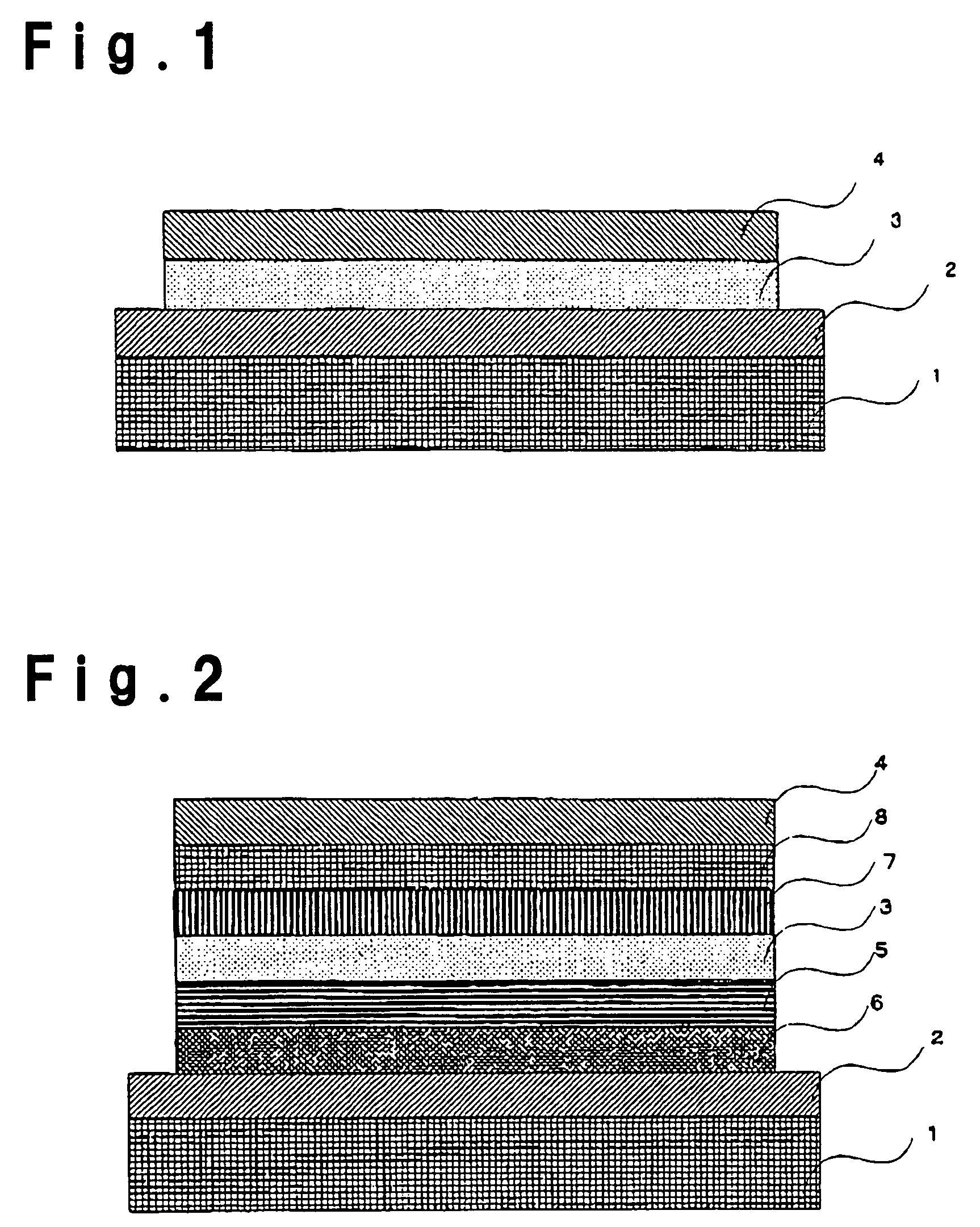
[0096]On a glass substrate, ITO was vapor-deposited in a thickness of 200 nm to form an anode 2 having a sheet resistance of 7Ω / □. On this anode 2, NPD represented by the formula (II) was vapor-deposited by a vacuum vapor deposition method to form a hole transport layer 5 having a film thickness of 60 nm. Then, on the hole transport layer, Alq of the formula (III) and coumarin 545T of the following formula (IV) were co-vapor-deposited by means of separate boats to form a light emitting layer 3 in a film thickness of 60 nm.

[0097]

[0098]The concentration of the coumarin 545T in the light emitting layer 3 was 1.0 mol %. On the light emitting layer, a layer of LiF having a thickness of 0.5 nm as an interface layer 8 and an aluminum layer having a thickness of 200 nm as a cathode 4 were vapor-deposited sequentially to prepare an organic EL display element as shown in FIG. 5. The vacuum degree at that time was 0.00107 Pa.

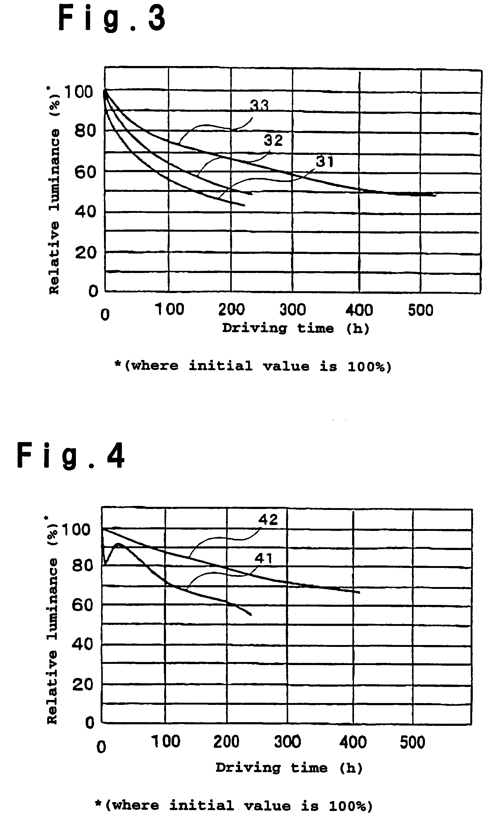
[0099]As aging to the organic EL display element, driving was...

case 2

[Case 2]

[0102]Operations up to the measurement of the emission luminance lifetime were carried out in the same manner as Case 1 except that aging after the formation of the films in Case 1 was not carried out. The change of the luminance per current density showed a monotonous reduction.

case 3

[Case 3]

[0103]Operations up to the measurement of the emission luminance lifetime were carried out in the same manner as Case 1 except that as the aging in Case 1, driving was carried out for 40 hours (at a frequency of 50 Hz) by repeating alternately the application of continuous 10 ms of a forward bias voltage of 12V and the application of continuous 10 ms without the application of bias voltage.

[0104]By the aging, the luminance per current density was 93% of the initial value. Subsequently, the change of the luminance per current density showed a monotonous reduction.


PUM

PropertyMeasurementUnit
Temperatureaaaaaaaaaa
Fractionaaaaaaaaaa

Abstract

A method for aging an organic electroluminescence display element where the integration value with respect to an applied voltage and a voltage application time in a reverse direction is at least twice as much as in a forward direction.

Description

BACKGROUND OF THE INVENTION[0001]1. Field of the Invention[0002]The present invention relates to a method for producing an organic electroluminescence (hereinbelow, abbreviated as the organic EL) display element.[0003]2. Discussion of Background[0004]Along with the rapid progress in the technical developments in the information communication field in recent years, more expectations are placed on flat display devices instead of CRTs. Among them, an organic EL display element is excellent in the high response, visibility, luminance, etc. and various studies are being made thereon.[0005]The organic EL display element announced by Tang et al. of Eastman Kodak, U.S.A. in 1987 has a two-layered lamination structure of thin organic films wherein tris (8-quinolinolato) aluminum (hereinbelow, abbreviated as “Alq”) as represented by the below-mentioned formula (III) is used for a light emitting layer, by which a high luminance as 1000 cd / m2 was obtained by driving it with a low voltage of 10V...

Claims


Application Information

Patent Timeline
IPC IPC(8): H01J9/44H05B33/10H05B33/14C09K11/06H01L51/00H01L51/30H01L51/50H01L51/56
CPCH05B33/10H05B33/145H01L51/0059H01L51/0062H01L51/0081Y10S428/917H01L2251/568H01L51/56H10K85/649H10K85/631H10K85/324H10K71/861H10K71/00
Inventor TAKAHASHI, AKIRAKATO, NAOKIKOBUNE, SHINJI
Owner NIPPON SEIKI CO LTD
Why Eureka
Try Eureka