Organic electroluminescence device

a technology of electroluminescence device and electroluminescence discharge tube, which is applied in the direction of discharge tube/lamp details, luminescence screen of discharge tube, natural mineral layered products, etc., can solve the problems of shortening the lifetime of half luminance, shortening the lifetime of display, and large voltage increase, so as to prolong the lifetime and suppress short circuit

Active Publication Date: 2005-08-09
OPTREX CORP
View PDF8 Cites 30 Cited by
  • Summary
  • Abstract
  • Description
  • Claims
  • Application Information

AI Technical Summary

Benefits of technology

[0012]The present inventors have found it possible to attain suppression of short circuiting and prolongation of the lifetime simultaneously by using a polymer compound for a hole tr

Problems solved by technology

Further, the organic EL device is usually a device constituted by thin layers, whereby short circuiting between the anode layer and the cathode layer, or a leakage current, is likely to bring about a display defect or shortening of the lifetime.
However, among devices having high luminous efficiency, there are some, of which the half luminance lifetime is short, or some whereby the voltage increase is large during constant current driving.
However, even by using this method, no adequate extension of the lifetime can be attained, and a substantial improvement is still desired.
One of the causes for the large increase of the voltage and the quick decrease of the luminance, is considered to be accumu

Method used


Image

  • Organic electroluminescence device
  • Organic electroluminescence device
  • Organic electroluminescence device

Examples


example 1

Present Invention

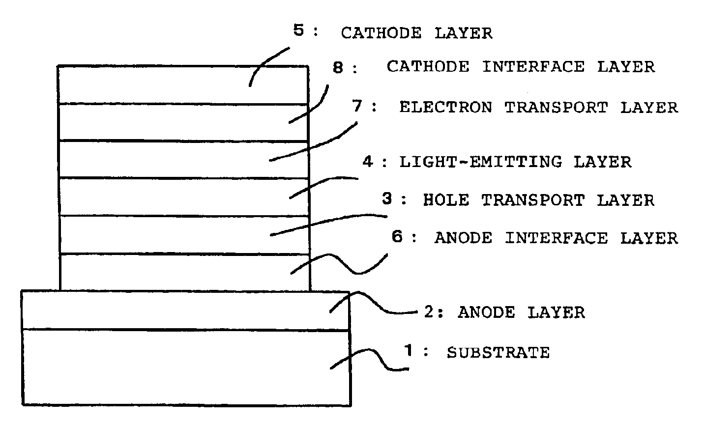
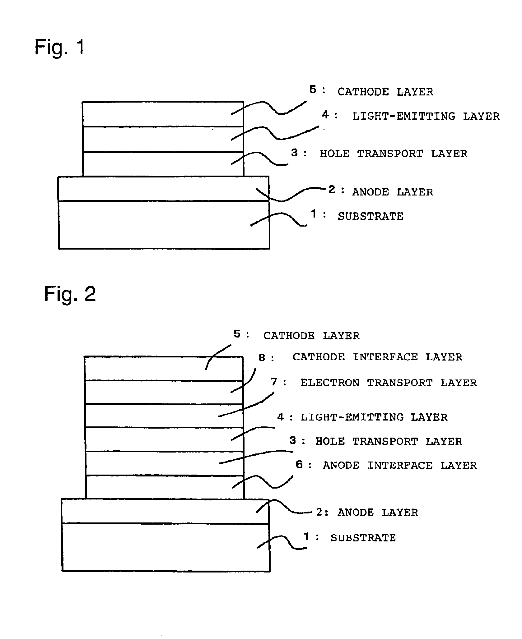
[0087]On a glass substrate, ITO was vapor-deposited in a thickness of 200 nm to form an anode layer 2 (sheet resistance: 7 Ω / □). A solution prepared by dissolving PPD of the following formula (8) (hereinafter referred to as the compound (8)) and a polyvinylcarbazole in a mass ratio of 1:2 in dichloromethane, was coated on the above anode layer 2 by a spin coating method, followed by drying to form an anode interface layer 6 having a thickness of 15 nm. Then, on the anode interface layer 6, the compound (8) was vapor-deposited in a thickness of 60 nm by a vacuum vapor deposition method to form a hole transport layer 3.

[0088]Then, Alq (host compound (A)) being the compound of the following formula (7), the compound (8) (guest compound (B)) and coumarin 545T of the following formula (9) (guest compound (C)) were, respectively, by means of separate boats, co-vapor-deposited in a thickness of 30 nm to form a light-emitting layer 4. The concentration of the compound (8) i...

example 2

Present Invention

[0091]A device was prepared and evaluated in the same manner as in Example 1 except that the construction of the light-emitting layer 4 in Example 1 was changed. Namely, Alq and coumarin 545T were, respectively, by means of separate boats, co-vapor-deposited in a thickness of 30 nm to form a light-emitting layer 4 (without using the compound (8)). The concentration of coumarin 545T in the light-emitting layer 4 was 1.0 mol %.

example 3

Present Invention

[0092]A device was prepared and evaluated in the same manner as in Example 1 except that the construction of the light-emitting layer 4 in Example 1 was changed. Namely, a light-emitting layer 4 was formed by using the same material as in Example 1 except that a compound of the following formula (10) (DCJTB) was used in an amount of 2 mol %, instead of coumarin 545T as the luminescent dye in the light-emitting layer 4 (the concentration of the compound (8) was 30 mol %). Here, DCJTB is a luminescent dye having a band gap which is smaller than the band gap of the host compound Alq.


PUM

PropertyMeasurementUnit
Percent by massaaaaaaaaaa
Glass transition temperatureaaaaaaaaaa
Energyaaaaaaaaaa

Abstract

An organic electroluminescence device comprising an anode layer, a cathode layer, a light-emitting layer present between the anode layer and the cathode layer, and a hole transporting thin film layer present between the light-emitting layer and the anode layer, wherein the hole transporting thin film layer in contact with the anode layer, contains at least 5 mass % of a polymer compound, and the value of the lowest unoccupied molecular orbit of the thin film layer is at least 2.1 eV.

Description

BACKGROUND OF THE INVENTION[0001]1. Field of the Invention[0002]The present invention relates to an organic electroluminescence device (hereinafter sometimes referred to also as an organic EL device) having improved emission characteristics and lifetime characteristics.[0003]2. Discussion of Background[0004]Along with the rapid progress in the technical developments in the information communication field in recent years, more expectations are placed on flat display devices as substitutes for CRT. Among them, an organic EL device is excellent in the high speed response, visibility, luminance, etc., and various studies are being made thereon.[0005]In an organic EL device, electron holes are injected from an anode, and electrons are injected from a cathode, whereby they will be recombined in a light-emitting layer to form excitons. Their energy will be transferred to a light-emitting material to emit light. In a case where the light-emitting layer is constituted by a host compound and ...

Claims


Application Information

Patent Timeline
IPC IPC(8): B32B19/00B32B9/00C09K11/06H01J63/00H01J63/04H01J1/62H01J1/00H05B33/14H05B33/22H01L51/00H01L51/30H01L51/50
CPCH01L51/5048H01L51/0052H01L51/0059H01L51/0062H01L51/0081H01L51/5012H10K85/649H10K85/631H10K85/615H10K85/324H10K50/14H10K50/11
Inventor TAKAHASHI, AKIRA
Owner OPTREX CORP
Why Eureka
Try Eureka