Directional ion etching process for patterning self-aligned via contacts

a technology of ion etching and patterning, which is applied in the direction of semiconductor devices, electrical equipment, basic electric elements, etc., can solve the problems of requiring fine precision and control, and affecting the quality of the material,

Active Publication Date: 2006-05-09
SAMSUNG ELECTRONICS CO LTD
View PDF6 Cites 144 Cited by
  • Summary
  • Abstract
  • Description
  • Claims
  • Application Information

AI Technical Summary

Problems solved by technology

Such etching or drilling requires fine precision and control, for too much etching or drilling may damage, deplete or entirely remove the underlying layer to which the via contact is intended to contact.
As the photoresist is a positive resist, the exposed area is made susceptible to decomposition upon contact with developer.
The process of creating the undercut photoresist mushrooms 200 whether by multiple masking, by using resists of different developing speeds, or a combination of both masking and different developing speeds is complex, time consuming and difficult.
Further, during the process of washing away the solid coated caps 204, it is possible that as they are solid structures they may collide with memory cells 208 damaging them immediately, or making them susceptible to premature failure.

Method used


Image

  • Directional ion etching process for patterning self-aligned via contacts
  • Directional ion etching process for patterning self-aligned via contacts
  • Directional ion etching process for patterning self-aligned via contacts

Examples


Embodiment Construction

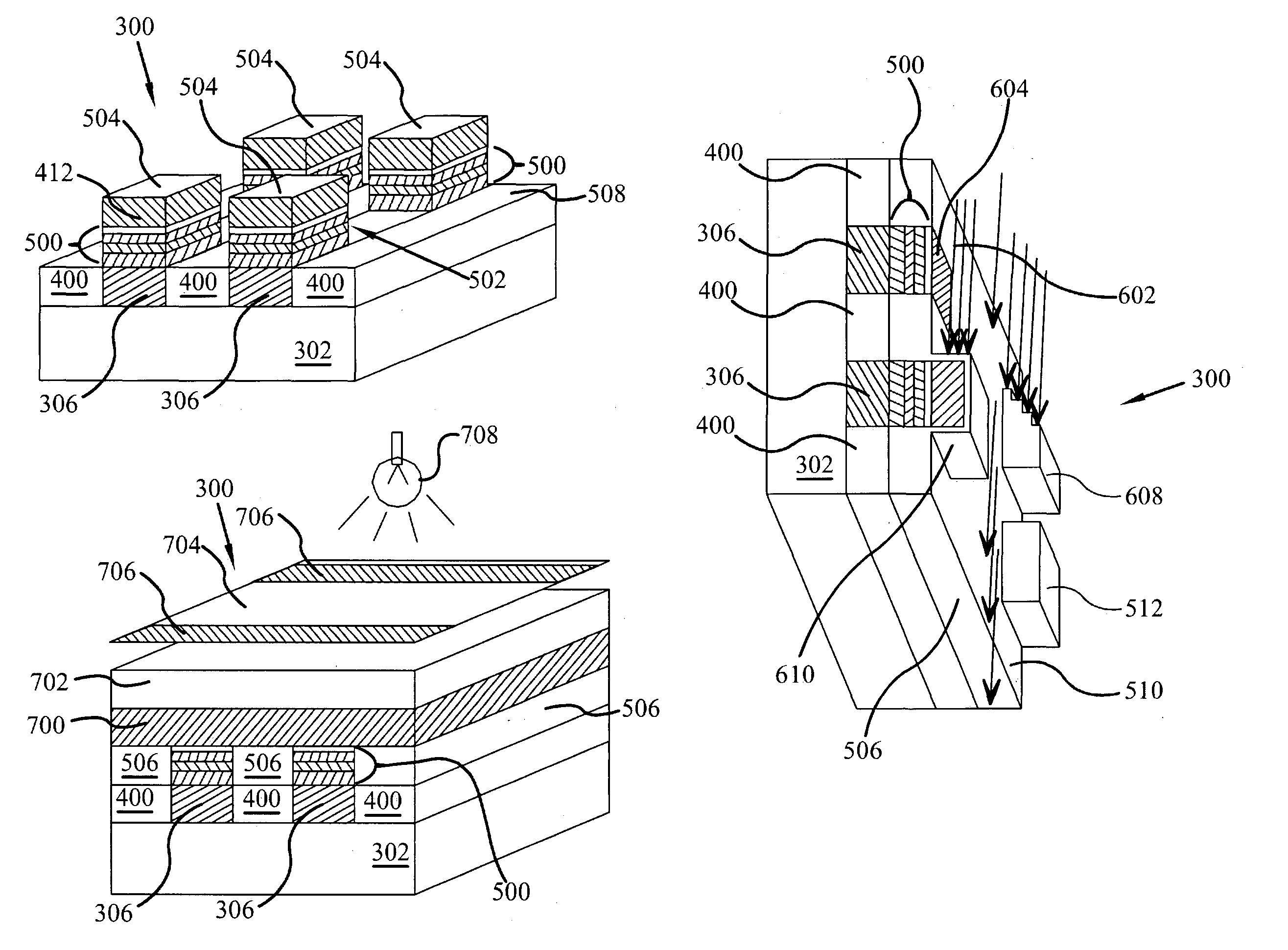
[0028]Before proceeding with the detailed description, it is to be appreciated that the present invention is not limited to use or application in conjunction with a specific type of semiconductor fabrication. Thus, although the present invention is, for the convenience of explanation, depicted and described with respect to typical exemplary embodiments relating to magnetic tunnel junction memory such as may be used for magnetic random access memory (MRAM), it will be appreciated that this invention may be applied with other types of semiconductor fabrication where self-aligned via contacts are desired.

[0029]Referring now to the drawings, FIGS. 3A through 5D conceptually illustrate a process of providing self-aligned via contacts in the fabrication of magnetic tunnel junction memory 300 according to an embodiment of the present invention. It will be appreciated that the described process need not be performed in the order in which it is herein described, but that this description is ...


PUM


Abstract

The invention provides a directional ion etching process to pattern self-aligned via contacts in the manufacture of semiconductor devices such as high density magnetic random access memory (MRAM). In a particular embodiment, a semiconductor wafer is prepared with vertically arranged layers, including a patterned layer in electrical contact with a conductive row layer. The patterned layer may be a magnetic tunnel junction layer. A photoresist is deposited on the junction layer, masked, exposed and developed. The non-protected junction layer is etched to provide appropriate junction stacks. The remaining photoresist caps are not dissolved, rather they and the surface of the wafer are coated with a dielectric. Directional ion etching at a low angle relative to the junction stack layer removes the coated photoresist caps and thereby provides at least one patterned self-aligned via contact.

Description

FIELD OF THE INVENTION[0001]This invention relates generally to the manufacture of semiconductor devices such as high density magnetic random access memory (MRAM) structures, and in particular to an improved method of patterning self-aligned via contacts using directional low angle ion etching.BACKGROUND OF THE INVENTION[0002]In many of today's micro-electronics, smaller more compact sizing yields greater speed and processing power. Improved materials and precision in manufacturing permit greater resolutions in semiconductor manufacturing.[0003]Generally speaking, semiconductors are manufactured through a layering process that provides two or more patterned conductive layers separated by intervening insulation layers. Considering the layers to be horizontally stacked, vertical points of contact between two or more conductive layers through the insulation layers are known as via structures, or more generally, via contacts. It is these via contacts that provide the wiring pattern for ...

Claims


Application Information

Patent Timeline
Patent Type & Authority Patents(United States)
IPC IPC(8): H01L21/44H01L21/60H01L27/22
CPCH01L27/222H01L21/76897H10B61/00
Inventor SHARMA, MANISH
Owner SAMSUNG ELECTRONICS CO LTD
Why Eureka
Try Eureka