Semiconductor device

a technology of semiconductor devices and semiconductors, applied in semiconductor devices, semiconductor/solid-state device details, electrical apparatus, etc., can solve the problems of increasing the area (size) of the substrate, increasing the manufacturing cost of the substrate, and difficult to form high-density wiring on the low-cost substrate. , to achieve the effect of low cost, high accuracy and fine structur

Inactive Publication Date: 2006-05-09
SOCIONEXT INC
View PDF7 Cites 0 Cited by
  • Summary
  • Abstract
  • Description
  • Claims
  • Application Information

AI Technical Summary

Benefits of technology

[0015]A more specific object of the present invention is to provide a semiconductor device in which bonding-wires can be applied parallel to each other to electrodes of high-speed signal lines when mounting a highly densified semiconductor element on a low-cost substrate while reducing a length of the bonding-wires.
[0023]According to the above-mentioned invention, the wiring path which requires impedance-matching is formed on the impedance-matched substrate so as to acquire impedance matching with high accuracy, while impedance matching with comparatively low accuracy is applied to other wiring paths. Accordingly, when mounting the semiconductor element having a fine pitch, a substrate having a relatively rough substrate structure is used and the impedance-matched substrate is used only for high-speed line requiring impedance matching, and, thereby, there is no need to make the entire substrate with a fine structure. Therefore, even when mounting a semiconductor element having a fine electrode pitch, a relatively inexpensive substrate can be used, which reduces a manufacturing cost of the semiconductor device.

Problems solved by technology

If a high-densification technique like a semiconductor element fabricating-technique is used for manufacturing a substrate on which a semiconductor element is mounted, a manufacturing cost of the substrate is increased.
It is difficult to form high-density wiring on the low-cost substrate, which increases an area (size) of a substrate.
Additionally, the terminals of the substrate are caused to apart away from the semiconductor element, which results in an increase in a length of each bonding-wire.
Especially, in a case in which high-speed signal lines are constituted by differential pairs, a length of bonding-wires is increased, which may result in a case where an appropriate impedance, for example, 100 Ω, cannot be provided.
Additionally, since the bonding-wires are elongated, there is a problem that it is difficult to take impedance-matching of bonding-wires with wiring formed in the low-cost substrate.

Method used


Image

  • Semiconductor device
  • Semiconductor device
  • Semiconductor device

Examples


Embodiment Construction

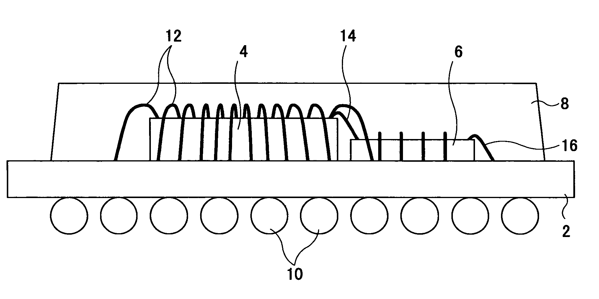
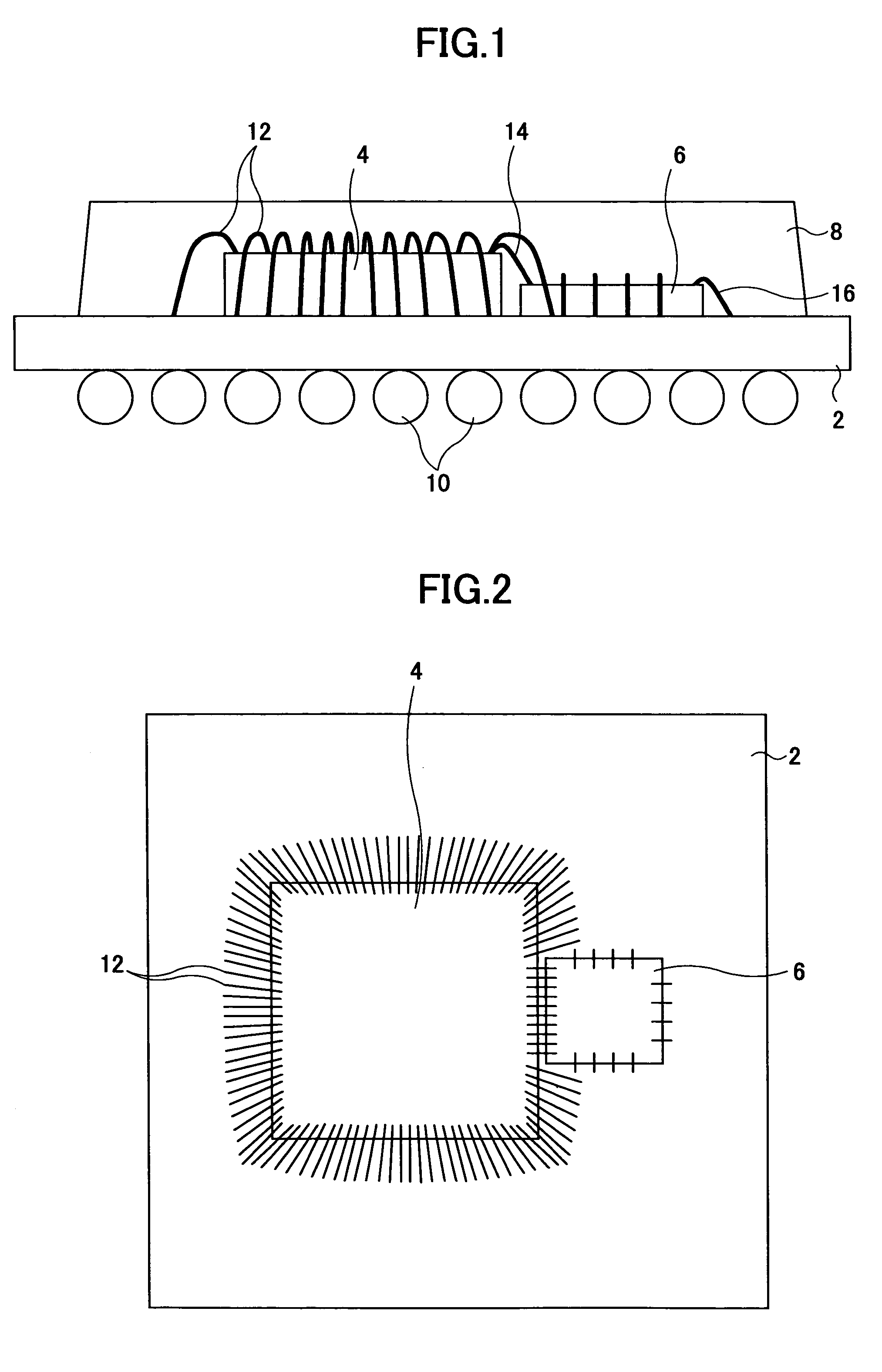
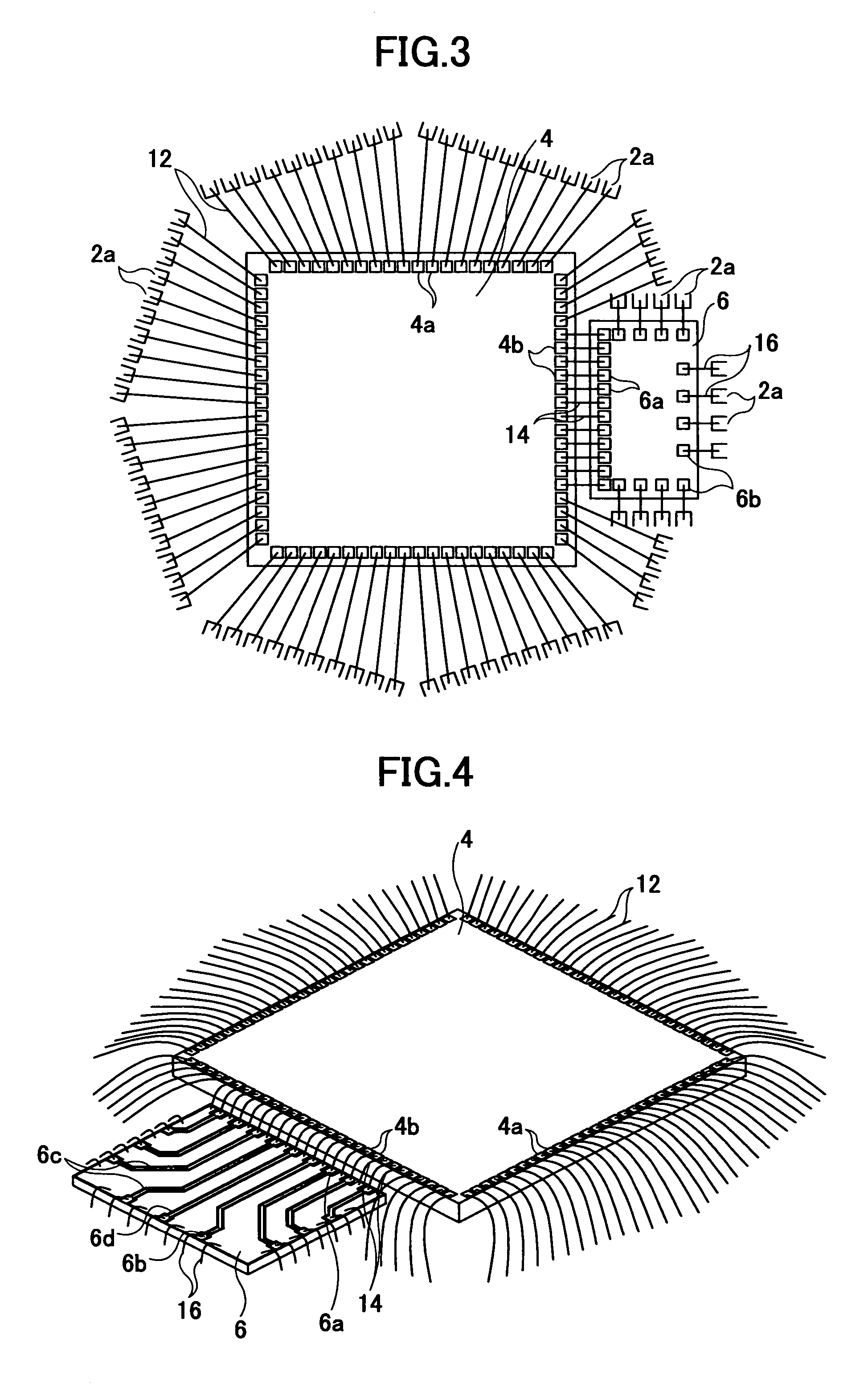
[0037]A description will now be given, with reference to FIGS. 1 through 3, of a semiconductor device according to a first embodiment of the present invention. FIG. 1 is an internal a see-through side view of a ball-grid array (BGA) type semiconductor device according to the first embodiment of the present invention. FIG. 2 is a see-through plan of the semiconductor device shown in FIG. 1. FIG. 3 is a plan view showing a structure of bonding-wires in the semiconductor device shown in FIG. 1.

[0038]The semiconductor device according to the first embodiment of the present invention comprises a substrate 2, a semiconductor element 4 mounted on the substrate 2 and an impedance-matched substrate 6 mounted on the substrate 2. The semiconductor element 4 and the impedance-matched substrate 6 are wire-bonded to electrodes 2a (refer to FIG. 3) of the substrate 2, and those are entirely encapsulated by a seal resin 8 on the substrate 2. Provided on the backside of the substrate 2 are solder ba...


PUM


Abstract

In a semiconductor device, bonding-wires can be applied parallel to each other to electrodes of high-speed signal lines when mounting a highly densified semiconductor element on a low-cost substrate while reducing a length of the bonding-wires. An impedance-matched substrate having wiring that impedance-matched with circuits of a semiconductor element is mounted on a substrate. A plurality of first metal wires connect between first electrodes of the semiconductor element and electrodes of the substrate. A plurality of second metal wires connect between second electrodes of the semiconductor element and first electrodes of the impedance-matched substrate. A plurality of third metal wires connect between second electrodes of the impedance-matched substrate and electrodes of the substrate. The second metal wires extend parallel to each other, and the third metal wires also extend parallel to each other.

Description

BACKGROUND OF THE INVENTION[0001]1. Field of the Invention[0002]The present invention relates to semiconductor devices and, more particularly, to a semiconductor device in which a semiconductor element is mounted on a substrate by wire-bonding.[0003]2. Description of the Related Art[0004]In recent years, high-densification of semiconductor element has progressed, which causes a reduction in a pitch of electrode terminals formed on an semiconductor element. Additionally, a processing speed of input and output signals has been increased, which results in, in many cases, provision of electrode terminals for inputting and outputting high-frequency signals.[0005]High-frequency signal lines connected to the electrode terminals for outputting and inputting high frequency signals need to take impedance-matching with peripheral circuits and wirings. Generally, a differential pair is formed by two high-frequency lines, and the differential pair is located between shielding lines such as a gro...

Claims


Application Information

Patent Timeline
Patent Type & Authority Patents(United States)
IPC IPC(8): H01L23/48H01L29/40H01L23/12H01L21/60H01L21/607H01L23/552H01L23/66
CPCH01L23/552H01L23/66H01L24/49H01L23/13H01L23/49838H01L2223/6627H01L2224/48011H01L2224/48091H01L2224/48137H01L2224/48227H01L2224/48465H01L2224/48471H01L2224/48475H01L2224/4912H01L2224/49171H01L2224/49175H01L2224/85051H01L2924/01002H01L2924/01004H01L2924/01006H01L2924/01029H01L2924/01033H01L2924/01078H01L2924/01082H01L2924/15311H01L2924/19011H01L2924/1903H01L2924/3011H01L2924/3025H01L24/48H01L2924/014H01L2924/00014H01L2924/00H01L24/45H01L2224/451H01L2924/15747H01L2924/181H01L2924/30111H01L2924/00012H01L23/12H01L23/48H01L21/60
Inventor TSUJI, KAZUTOKUBOTA, YOSHIHIROASADA, KENJIHOSOYAMADA, SUMIKAZU
Owner SOCIONEXT INC
Why Eureka
Try Eureka