Delay circuit and method

a delay circuit and delay technology, applied in the field of delay circuit and method, can solve the problems of delay in the signal that passes through the delay circuit and the inability to satisfy the timing relationship for every signal, and achieve the effect of suppressing the delay time and not increasing the delay time excessively

Inactive Publication Date: 2006-05-09
RENESAS ELECTRONICS CORP
View PDF25 Cites 17 Cited by
  • Summary
  • Abstract
  • Description
  • Claims
  • Application Information

AI Technical Summary

Benefits of technology

[0013]The present invention is provided in view of the background situation described above, and it is an object of the present invention to provide a delay circuit and a method of delaying logic signals that do not lead to excessive increase in the delay time even if the source voltage drops, so as to enable to control the delay time from increasing.
[0027]That is, in the present delay circuit that delays a logic signal having two logic levels consisting of a low level and a high level, because the delay circuit is designed in such a way that the delay times are different for the high and low levels and the delay circuitry targets a logic level having a shorter delay time as the delay target, the delay time is not increased excessively even if the source voltage drops, thereby suppressing the delay time from increasing.

Problems solved by technology

According to the delay circuit based on the conventional technology, because the n-MOS transistors JN1˜JN4 form MOS capacitors and capacitive loads are connected to each of the inverters, changes in the output signals from each inverter are successively moderated, thereby creating delays in the signal that passes through the delay circuit.
However, according to the delay circuit in the conventional technology described above, when the source voltage is decreased, delay times are increased excessively relative to the delay times in normal logic circuitries, resulting in a problem that the timing relationships are not satisfied for every signal.
The result is a shift in timing between the signal transmitted through the internal logic circuits and the signal transmitted through the delay circuit, which can lead to occasional erroneous operation of those circuits that depend on timely receiving of such signals.

Method used


Image

  • Delay circuit and method
  • Delay circuit and method
  • Delay circuit and method

Examples


embodiment 1

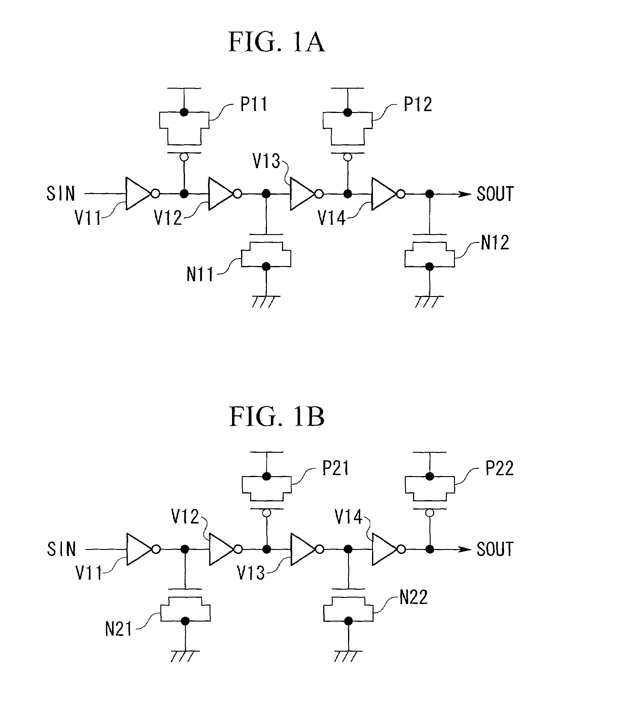
[0048]FIG. 1A shows a delay circuit in Embodiment 1.

[0049]This delay circuit is designed to output signal OUT by delaying a logic signal SIN that has two logic levels consisting of low level and high level, and exhibits a characteristic that the delay time for a logic signal input at the high level is different than a logic signal input at the low level, so that the delay circuit is comprised of a delaying system such that, of the two logic levels (low and high logic levels) given as the logic levels of the logic signal SIN, the logic level targeted for delay is the one having a shorter delay time. In the example shown in the diagram, the high level of the logic signal SIN is the delay target so that the logic signal SIN is delayed when the logic signal SIN changes from the low level to the high level.

[0050]The structure of the delay circuit will be explained in the following.

[0051]As shown in FIG. 1A, this delay circuit is comprised by an inverter chain that includes inverters V11˜...

embodiment 2

[0067]Embodiment 2 will be explained in the following.

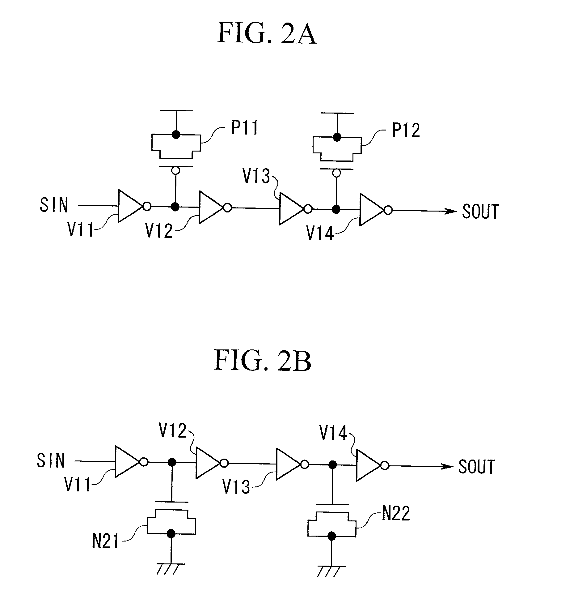
[0068]FIG. 2 shows a structure of a delay circuit in Embodiment 2.

[0069]In Embodiment 1 described above, the delay circuit depends on a MOS capacitor comprised by a p-MOS transistor in the output section of an inverter whose output signal changes from the high level to the low level according to the nature of a logic signal SIN, and on an n-MOS capacitor comprised by an n-MOS transistor in the output section of an inverter whose output signal changes from the low level to the high level, but in Embodiment 2, an MOS capacitor is provided in either the output section of an inverter whose output signal changes from the high level to the low level or the output section of an inverter whose output signal changes from the low level to the high level according to the nature of a logic signal SIN.

[0070]FIG. 2 shows an example of the structure of the delay circuit in Embodiment 2.

[0071]The example shown in FIG. 2A, n-MOS transistors N11, ...

embodiment 3

[0075]Embodiment 3 will be explained in the following.

[0076]FIG. 3 shows a structure of a delay circuit in Embodiment 3.

[0077]In the example shown in the diagram, p-MOS transistors P11, P12 shown in FIG. 1A to serve as the MOS capacitors are replaced with n-MOS transistors N31, N32 of high-Vt, and n-MOS transistors N11, N12 are replaced with p-MOS transistors 31, P32 of high-Vt.

[0078]Here, the drain and source of n-MOS transistors N31 are connected in common to the output section of the inverter V11, and the drain and source of n-MOS transistor N32 are connected to the output section of the inverter V13, and the gate terminals of n-MOS transistors N31, N32 are both fixed at the source voltage VDD. Also, the drain and source of p-MOS transistor P31 are connected to the output section of the inverter V12, and the drain and source of p-MOS transistor P32 are connected to the output section of the inverter V14, and the gate terminals of the p-MOS transistors P31, P32 are both fixed at t...


PUM


Abstract

A delay circuit does not lead to excessive increase in the delay time even if the source voltage drops, and enables to control the delay time from increasing. The delay circuit is designed to delay a logic signal SIN having two logic levels consisting of a low level and a high level, such that the delay times are different for the high and low levels, and the circuit chooses either the low level or the high level and targets a logic level having a shorter delay time. That is, n-MOS transistors N11, N12 and p-MOS transistors P11, P12 are provided as MOS capacitors, so as to change from the off-state to the on-state during the transition period of a signal that appears on each node disposed on a delay path of logic signals. Such a circuit design enables to control source-voltage dependence of delay time so that, even if the source voltage drops, delay times are not increased excessively.

Description

BACKGROUND OF THE INVENTION[0001]1. Field of the Invention[0002]The present invention relates to a delay circuit and a method for delaying a logic signal having two logic levels, high and low levels, and relates in particular to a technology for suppressing the dependence of the delay time on source-voltage.[0003]2. Description of the Related Art[0004]Conventionally, in semiconductor apparatuses, delay circuits are used for obtaining timing for signals that are necessary for operating various circuits.[0005]FIG. 16 shows an example of a circuit structure of a delay circuit according to the conventional technology.[0006]The circuit shown in the diagram is constructed by forming an inverter chain using a plurality of inverters JV1˜JV4, and connecting an n-MOS transistor JN1˜JN4 between the output section of each of the inverter JV1˜JV4 and the ground. The gate terminals of the n-MOS transistors JN1˜JN4 are connected to the output section of the respective inverters JV1˜JV4, and the so...

Claims


Application Information

Patent Timeline
Patent Type & Authority Patents(United States)
IPC IPC(8): H03H11/26G11C8/00G11C11/4076H03K5/00H03K5/14
CPCH03K5/133H03K2005/0013G11C8/00
Inventor TAKAHASHI, HIROYUKI
Owner RENESAS ELECTRONICS CORP
Why Eureka
Try Eureka