Semiconductor device, sales method for semiconductor device, sales system for semiconductor device and program product storing sales program for semiconductor device

Inactive Publication Date: 2006-05-09
KK TOSHIBA
View PDF10 Cites 0 Cited by
  • Summary
  • Abstract
  • Description
  • Claims
  • Application Information

AI Technical Summary

Benefits of technology

[0018]In an aspect of the present invention, there is provided a sales method for selling semiconductor devices by way of a communication network, the method comprising: presenting function-related information and price-related information on partially good semiconductor devices having one or more than on

Problems solved by technology

In the course of development, however, some of the memory cells of a memory product can become defective due to one or more than one problems in the manufacturing process.
Then, the memory chip cannot be produced with the designed memory size.
Then, it is no longer possible to develop and market the chip as semiconductor memory device having an ECC function.
Therefore, the circuit system is not designed for a total shutdown of the parity bit circuit and a chip information rewriting operation (e.g., information on the presence or absence of an ECC function).
Thus, the chip cannot be classified as perfectly good product having no ECC function.
However, there may be cases where a defect is found outside the parity cell regions or the chip cannot find any particular application.
However, such a technique of excluding the ECC function and reducing the memory size will not remarkably improve the manufacturing yield.
Then, under the current circumstances, the chip will completely lose its market value although three out of the four cell arrays operate without any problem.
Of course, like the earlier discussion, it may not become a perfectly good product if it is made to apparently have no ECC function because the circuit system is not modified.
However, because of the market practice of selling and buying semiconductor products on a lot basis, there is no knowing who want to buy such imperfect products and all such attempts have failed so far.
However, partially good products are not perfectly good products and, under the current circumstances, there is no knowing who want to buy partially good products.
Therefore, to date, such partially good products are simply wasted to make the semiconductor manufacturer partly miss the expected profit.
On the other hand, from the viewpoint of buyers of semiconductor devices, who may be computer manufacturers, memory devices having an unnecessarily large memory capacity simply push up the prices of their products.
Then, a 128 mega-bit memory will not do but the memory capacity of a 256 mega-bit memory is too much.
However, no memories with a memory capacity between 128 mega bits and 256 mega bits are commercially available.
However, there is no knowing which semiconductor manufacturer is selling such an imperfect product.

Method used


Image

  • Semiconductor device, sales method for semiconductor device, sales system for semiconductor device and program product storing sales program for semiconductor device
  • Semiconductor device, sales method for semiconductor device, sales system for semiconductor device and program product storing sales program for semiconductor device
  • Semiconductor device, sales method for semiconductor device, sales system for semiconductor device and program product storing sales program for semiconductor device

Examples


first embodiment

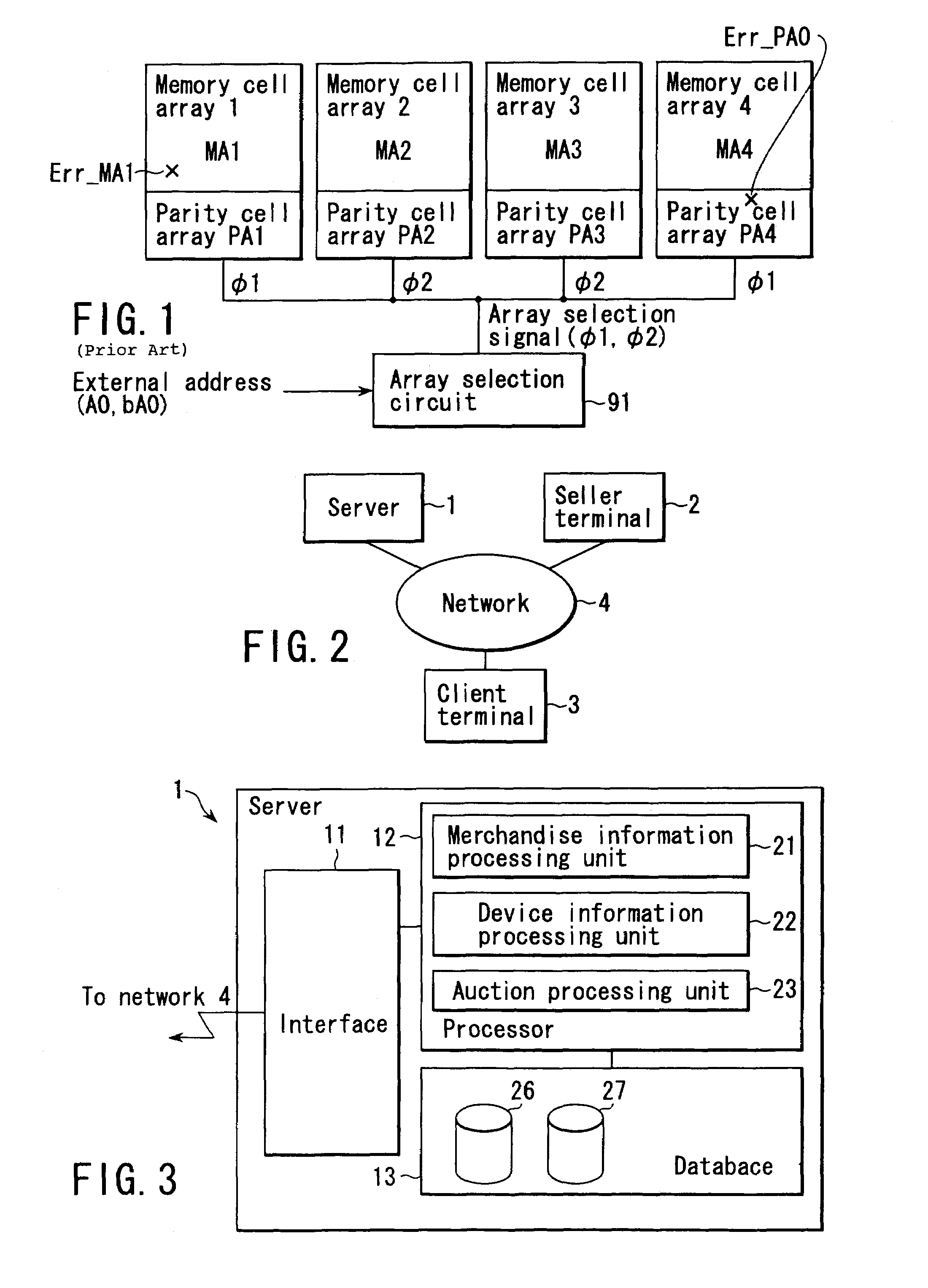
[0037]FIG. 2 is a schematic illustration of the configuration of a communication network to be used for the first embodiment of a system for selling semiconductor devices according to the invention. In FIG. 2, a server 1, a seller terminal 2 and a client terminal 3 are connected to the network 4. The server 1 executes a computer program for successfully concluding transactions of selling and buying semiconductor devices. The seller terminal 2 is dedicated to the seller who manufactures and wants to sell partially good semiconductor devices. The client terminal 3 is dedicated to a client who wants to buy one or more than one partially good semiconductor devices from the semiconductor device seller. While only a single seller terminal 2 and a single client terminal 3 are shown in FIG. 2, normally a plurality of sellers and a plurality of clients are connected to the network 4.

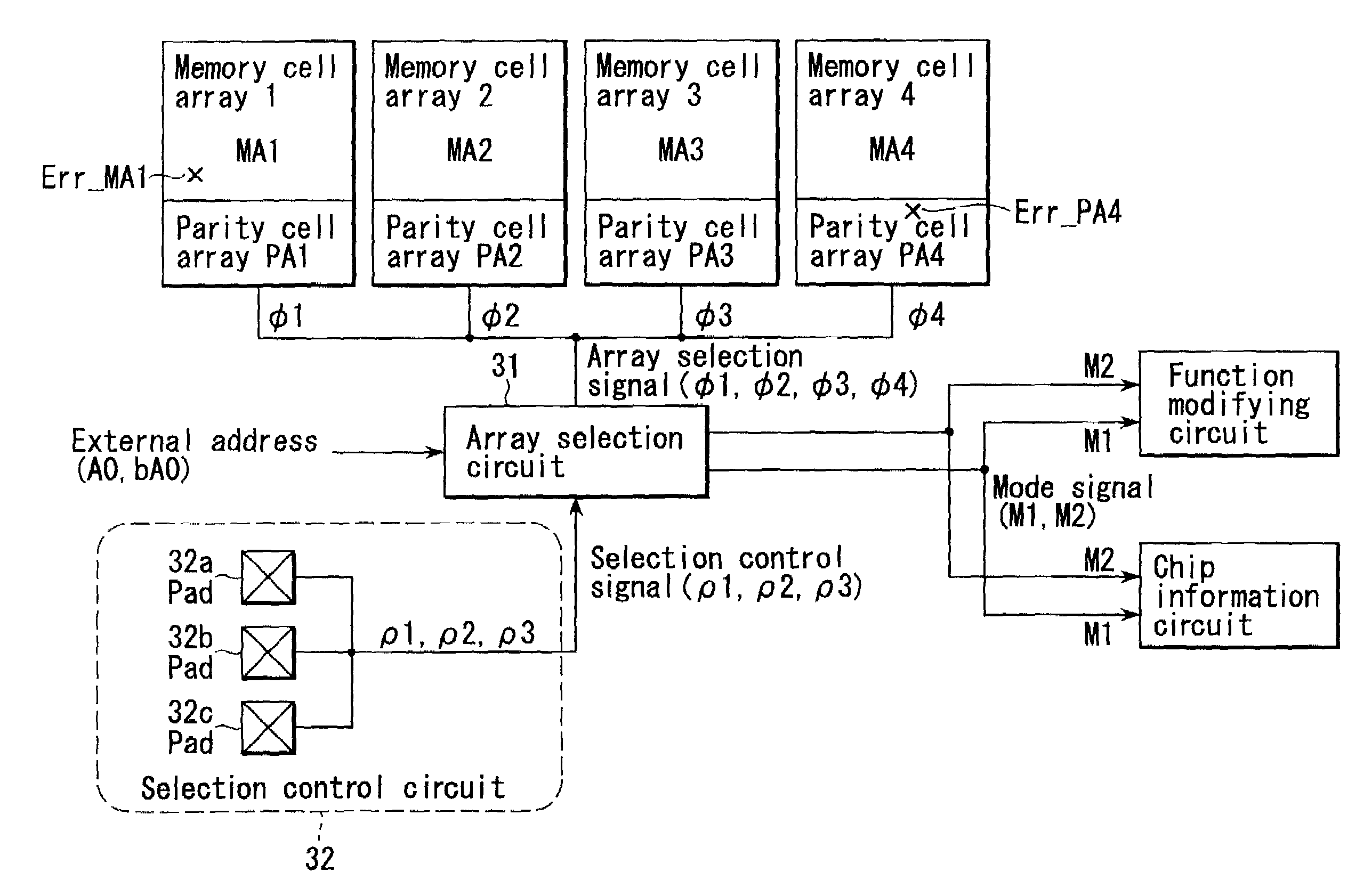
[0038]FIG. 3 is a schematic block diagram of a possible configuration of the server of the first embodiment. A...

second embodiment

[0088]This embodiment is realized by modifying the first embodiment, which is a semiconductor memory device adapted to be sold by way of a communication network. This embodiment of semiconductor memory device is characterized in that the selection control circuit is realized by using laser fuses. The basic configuration of this embodiment is same as that of the first embodiment. Therefore, this embodiment will be described only in terms of the difference between this embodiment and the first embodiment. The components of this embodiment that are same as or similar to those of the first embodiment are denoted respectively by the same reference symbols.

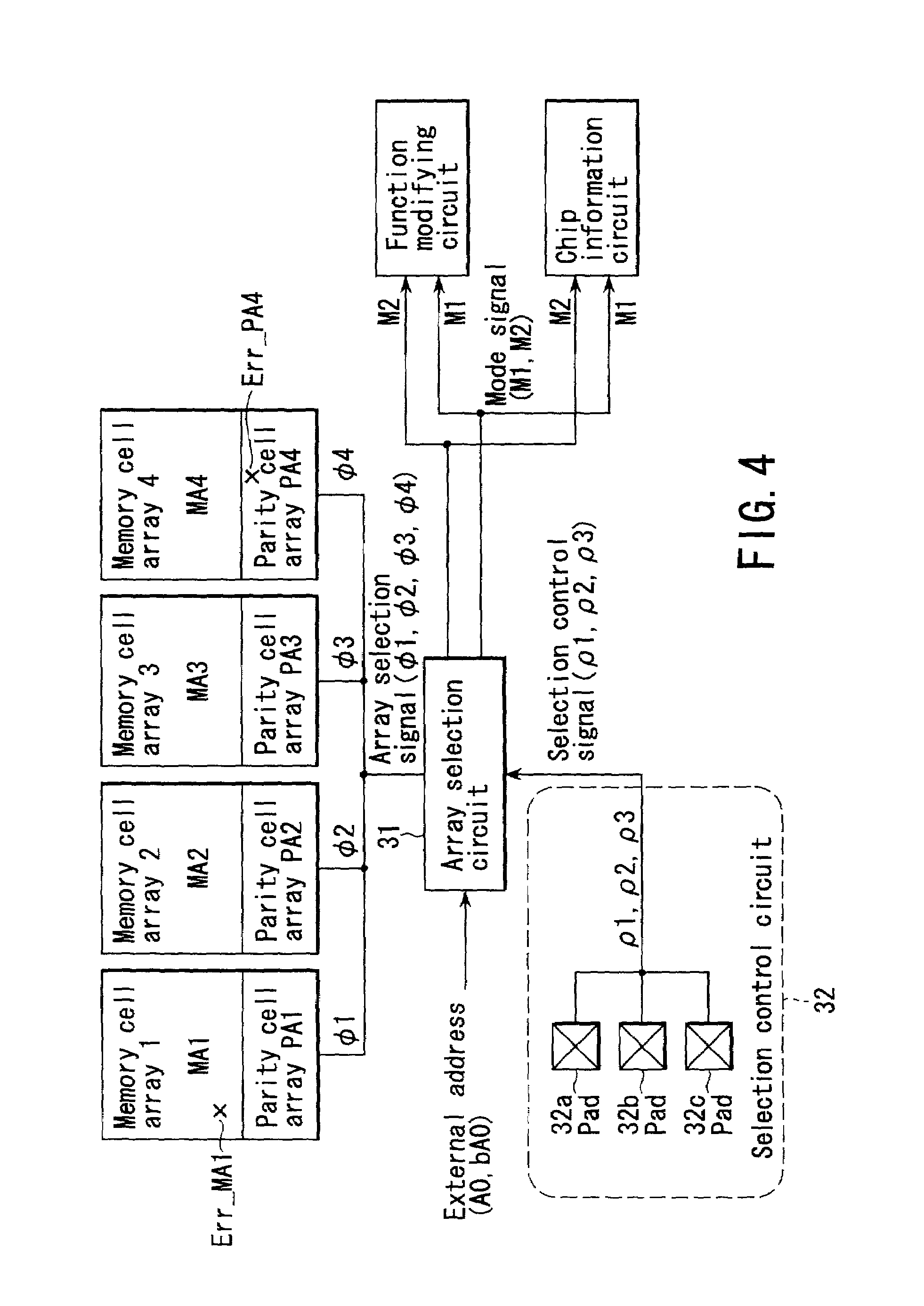
[0089]FIG. 10 is a schematic block diagram of the second embodiment of semiconductor device according to the invention and corresponds to FIG. 4 illustrating the first embodiment. As shown in FIG. 10, the selection control circuit 32 comprising pads 32a through 32c of the first embodiment is replaced by a selection control circuit 112 c...

third embodiment

[0092]This embodiment is realized by modifying the first embodiment, which is a semiconductor memory device adapted to be sold by way of a communication network. This embodiment of semiconductor memory device is characterized in that the selection control circuit is realized by using electric fuses. The basic configuration of this embodiment is same as that of the first embodiment.

[0093]FIG. 11 is a schematic block diagram of the third embodiment of semiconductor device according to the invention and corresponds to FIG. 4 illustrating the first embodiment. As shown in FIG. 11, the selection control circuit 32 comprising pads 32a through 32c of the first embodiment is replaced by a selection control circuit 122 comprising electric fuses 122a through 122c in this embodiment.

[0094]Each of the electric fuses 122a through 122c is a fuse that can be electrically broken so as to control the signal level of the corresponding one of selection control signals ρ1 through ρ3. For instance, sele...


PUM


Abstract

A semiconductor device includes a plurality of cell arrays, a selection control circuit to generate and to output a selection control signal. An array selection circuit generates internal address signals on the basis of an external address signal and the selection control signal. The array selection circuit outputs the internal address signals to the plurality of cell arrays to select ones of the cell arrays. A sales method for selling semiconductor devices includes presenting function-related information and price-related information on partially good semiconductor devices to client terminals and prompting the client terminals to provide purchase / non-purchase information and determining the possibility of successful transactions on the basis of the purchase / non-purchase information. A sales system for selling semiconductor devices uses the sales method and a sales program product for causing a computer system to sell semiconductor devices using the sales method.

Description

CROSS-REFERENCE TO RELATED APPLICATIONS[0001]This application is based upon and claims the benefit of priority from the prior Japanese Patent Application No. 2000-297447, filed Sep. 28, 2000, the entire contents of which are incorporated herein by reference.BACKGROUND OF THE INVENTION[0002]1. Field of the Invention[0003]This invention relates to a sales method for selling partially good semiconductor products by way of a communication network, a sales system for semiconductor devices, a recording medium storing a sales program for semiconductor devices and a rejected semiconductor device adapted to operates as partially good device.[0004]2. Description of the Related Art[0005]General purpose memories are normally designed to comprise a plurality of memory cell arrays in order to reduce the length and hence the capacity of each bit line and / or lower the power consumption rate of the memory. A memory comprising a plurality of memory cell arrays is produced by way of a memory cell arra...

Claims


Application Information

Patent Timeline
IPC IPC(8): G11C8/00G06Q30/06G06Q30/08G06Q50/00G11C29/00G11C29/04
CPCG06Q30/06
Inventor ARIKADO, TSUNETOSHIOKUMURA, KATSUYAYONEYA, KAZUHIDEKOYANAGI, MASARU
Owner KK TOSHIBA
Why Eureka
Try Eureka