Semiconductor package and method for manufacturing the same

Active Publication Date: 2006-05-16
AMKOR TECH SINGAPORE HLDG PTE LTD
View PDF5 Cites 29 Cited by
  • Summary
  • Abstract
  • Description
  • Claims
  • Application Information

AI Technical Summary

Benefits of technology

[0012]Since, according to the present invention, the posts have two parts, a first, or inner, post and second, or outer, post, the strength of the post is greater than that of a conventional solder ball. Consequently, the post has superior endurance, reliability and lifetime. In addition, since each of the first, or inner, posts and the second, or outer, posts may be used as an individual signal line, a greater number of signal lines can be formed. Accordingly, a greater number of I/O counts can be formed in a semiconductor die created in accordance with the present invention.
[0013]In addition, if the second, or outer, post

Problems solved by technology

Consequently, there is a physical lim

Method used


Image

  • Semiconductor package and method for manufacturing the same
  • Semiconductor package and method for manufacturing the same
  • Semiconductor package and method for manufacturing the same

Examples


Embodiment Construction

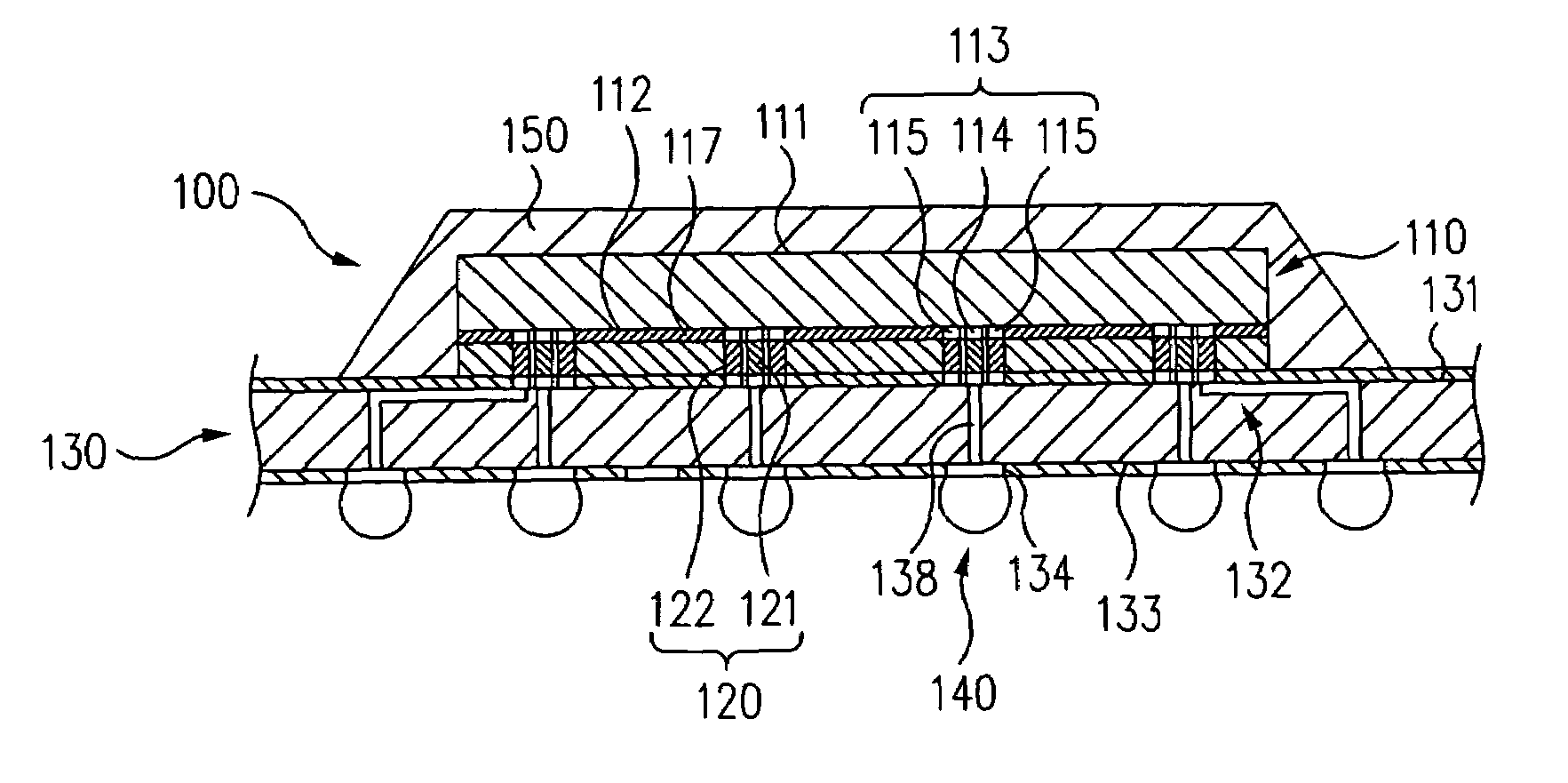
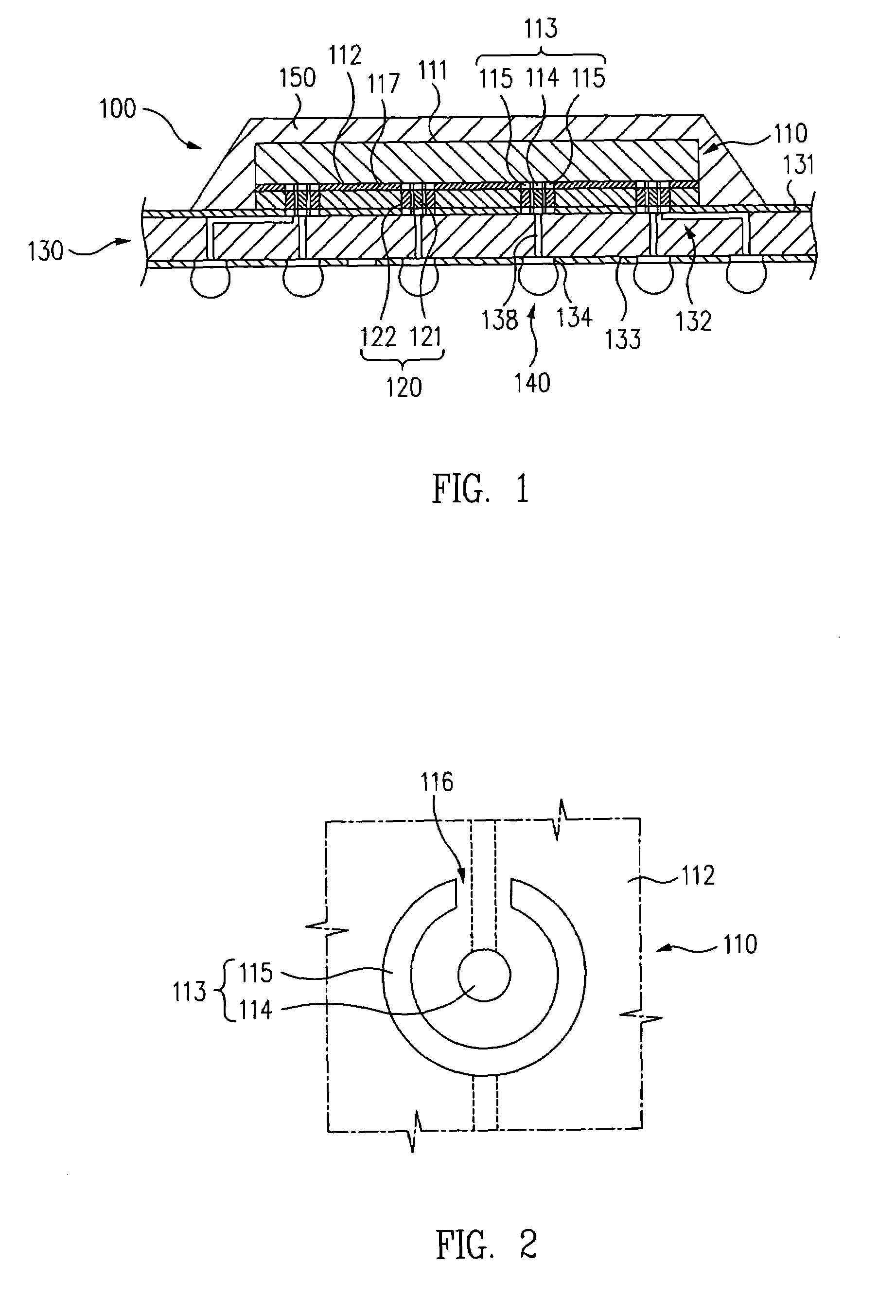
[0023]FIG. 1 shows a sectional view of a flip-chip assembly package 100 according to one exemplary embodiment of the present invention.

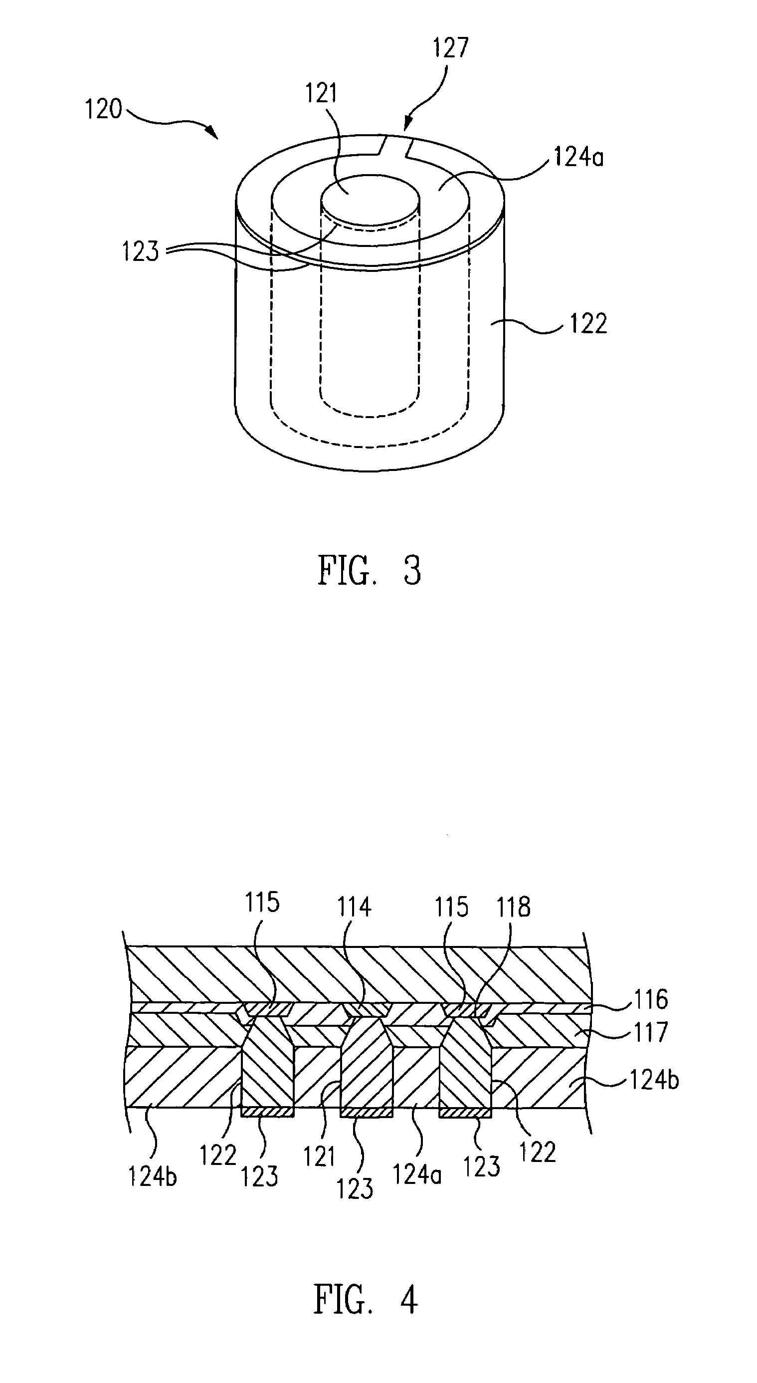
[0024]As shown in FIG. 1, flip-chip assembly package 100 according to the present invention includes a semiconductor die 110, a plurality of posts 120 formed respectively in a plurality of bond pads 113 of the semiconductor die 110, a substrate 130 having electrically conductive patterns 132 and 134 bonded to end portions of posts 120, and a plurality of solder balls 140 welded to a lower surface of substrate 130. In addition, flip-chip assembly package 100 has an encapsulant 150 formed on an upper surface of substrate 130 and surrounding semiconductor die 110 and posts 120.

[0025]Semiconductor die 110 has a first surface 111 having an approximately planar shape and a second surface 112 formed in opposition to first surface 111 and having an approximately planar shape. Second surface 112 of semiconductor die 110 is formed with bond pads 113. Bond pads...


PUM


Abstract

A semiconductor package, and a method for fabricating the semiconductor package, includes a semiconductor die having a plurality of bond pads including a first bond pad positioned at a center of the bond pad and formed at a first surface of the semiconductor die and a second bond pad spaced from the first bond pad by a predetermined distance while surrounding the first bond pad. The semiconductor package includes first and second posts formed on the bond pads of the semiconductor die and a substrate formed with electrically conductive patterns corresponding to the bond pads of the semiconductor die and bonded to the post.

Description

FIELD OF THE INVENTION[0001]The present invention relates to semiconductor packages having high pin counts and a method for their manufacture.BACKGROUND OF THE INVENTION[0002]Recently, manufacturers have started using PCB (Printed Circuit Board) to replace lead frames in semi-conductor packages to reduce inductance, improve electrical performance, improve heat-emission performance and improve surface-mounting performance for the semiconductor package.[0003]When the PCB used in the semiconductor package includes a thermosetting resin layer, which is a base layer, a plurality of copper wiring patterns are formed on upper and lower surfaces of the base layer, and a solder mask coating is formed on the copper wiring patterns.[0004]In order to form the semiconductor package by mounting a die on the PCB, a solder ball is welded between the copper wiring patterns of the PCB and a bonding pad of the die such that the copper wiring patterns are electrically connected to the bonding pad of th...

Claims


Application Information

Patent Timeline
IPC IPC(8): H01L23/48H01L23/52H01L29/40
CPCH01L23/3128H01L23/49838H01L23/66H01L24/03H01L24/05H01L24/11H01L24/12H01L24/16H01L23/49811H01L2224/16235H01L2223/6622H01L2224/0401H01L2224/05599H01L2224/1147H01L2224/13099H01L2224/16225H01L2924/01013H01L2924/01022H01L2924/01028H01L2924/01029H01L2924/01047H01L2924/01078H01L2924/01079H01L2924/01082H01L2924/014H01L2924/14H01L2924/15311H01L2924/30107H01L2924/3011H01L2924/3025H01L2924/01033H01L2924/00014H01L2224/13022H01L2224/16238
Inventor PAEK, JONG SIKLEE, KWANG EUNGLEE, SEUNG JU
Owner AMKOR TECH SINGAPORE HLDG PTE LTD
Why Eureka
Try Eureka