
Method and device for switching on and off power semiconductors, especially for the torque-variable operation of an asynchronous machine, for operating an ignition system for spark ignition engines, and switched-mode power supply

a technology of power semiconductors and switching devices, which is applied in the direction of transistors, pulse generators, electrical apparatus, etc., can solve the problems of affecting the operation performance of the collector-emitter, the voltage vs. time dusub>ce/sub>/dt must be limited, and the excess voltage at the igbt. to achieve the effect of reducing the cost of operation

Inactive Publication Date: 2006-05-16
RUBITEC GES FUR INNOVATION & TECH DER RUHR UNIV BOCHUM
View PDF14 Cites 14 Cited by
  • Summary
  • Abstract
  • Description
  • Claims
  • Application Information

AI Technical Summary

Benefits of technology

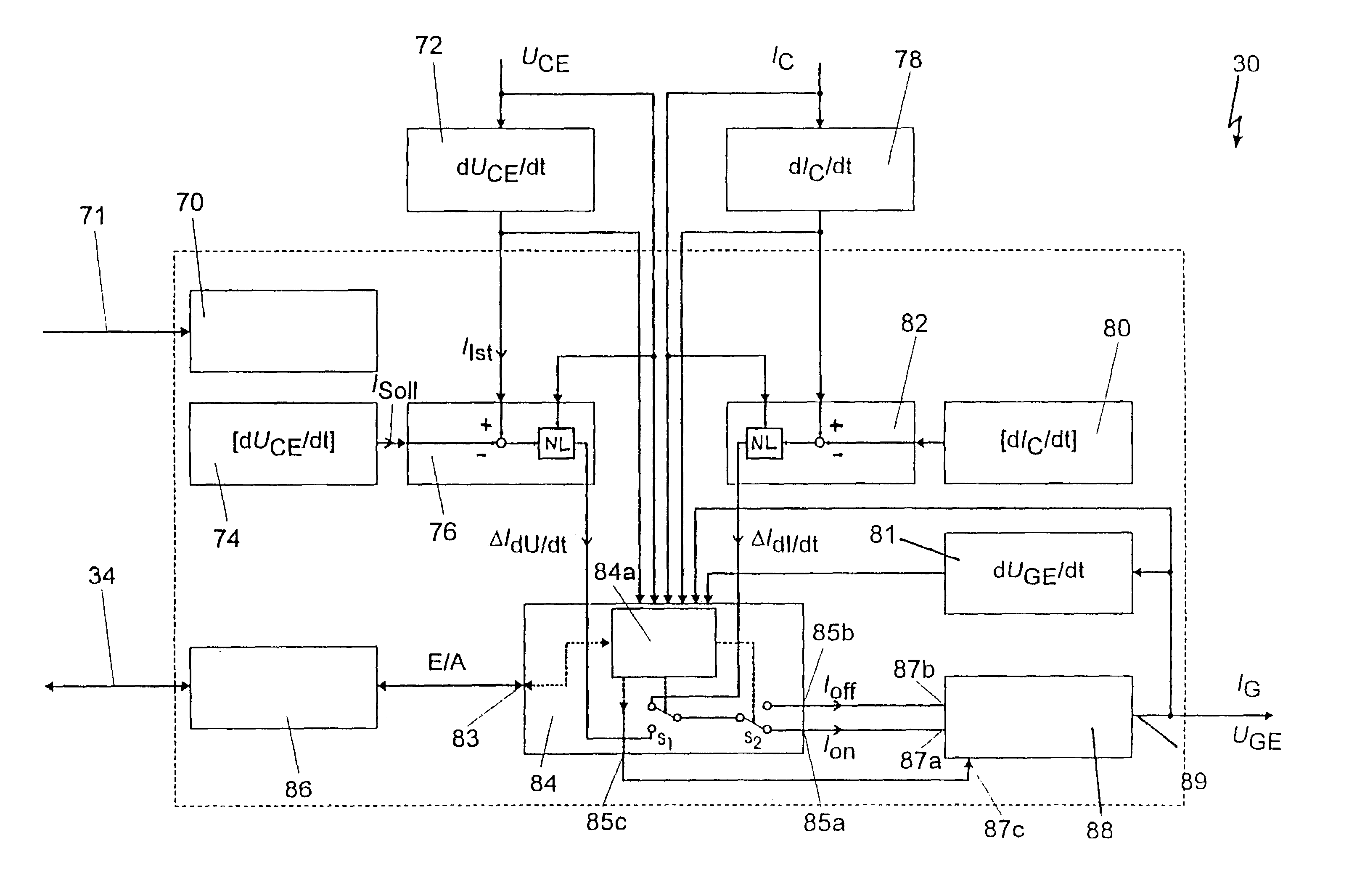
[0108]All these measures and the criteria have the advantage to exactly determine the moments in time when the switching-over from the control of the one parameter to the control of the respective other parameter shall be effected.
[0147]This embodiment of the circuitry enables the implementation of the various methods discussed in detail above, and further has the advantages of a high safety against interferences at low control voltages, as will be described below in further detail.

Problems solved by technology

On the other hand, the edge steepness of the two afore-mentioned variable quantities may not be selected too high, because in practice there exist limiting side conditions.
For example, the variation of the collector-emitter voltage vs. time dUCE / dt must be limited because otherwise inadmissibly high displacement currents appear within the isolation of the motor.
Finally, a too high time variation dIC / dt of the collector current in connection with the parasitic inductance could cause an excess voltage at the IGBT.
This concept, however, has the disadvantage that the resistor or the resistors, respectively, may only be dimensioned according to the power semiconductor data sheet, wherein changes in the operational conditions (e.g. varying temperature), as well as in particular variations in the load may result in partially drastical deteriorations of the operational performance.
Moreover, the two functions are approximately highly non-linear and do not show a constant dUCE / dt and dIC / dt which, however, would be desirable due to the load on the isolation and the electromagnetic radiation.
This generally requires a higher voltage class of the IGBT and, therefore, additional costs.
Another disadvantage of prior art drive circuits consists in that the maximum values of dUCE / dt and dIC / dt only appear over a short period of time during the switching process.
Finally, conventional drive circuits have the disadvantage that certain components determining the transient behavior are partially located ahead of the gate and partially at the IGBT output.
These components are, therefore, exposed to high voltage.
This results in high currents, and, therefore, power components at additional costs are required.
This prior art power output stage allows an independent setting within the two control circuits of the current signal and the voltage signal, however, no close loop-control starting from a predetermined desired value is used, so that the current function on the one hand and the voltage function on the other hand may not be controlled individually.
Further, it is indicated that both an open-loop control or a close-loop control might be used, however, there is no enabling disclosure how this could be done in practice because the given examples are inoperative and the associated description is incorrect.
Therefore, no continuous close-loop control is provided.

Method used


Image

  • Method and device for switching on and off power semiconductors, especially for the torque-variable operation of an asynchronous machine, for operating an ignition system for spark ignition engines, and switched-mode power supply
  • Method and device for switching on and off power semiconductors, especially for the torque-variable operation of an asynchronous machine, for operating an ignition system for spark ignition engines, and switched-mode power supply
  • Method and device for switching on and off power semiconductors, especially for the torque-variable operation of an asynchronous machine, for operating an ignition system for spark ignition engines, and switched-mode power supply

Examples


Embodiment Construction

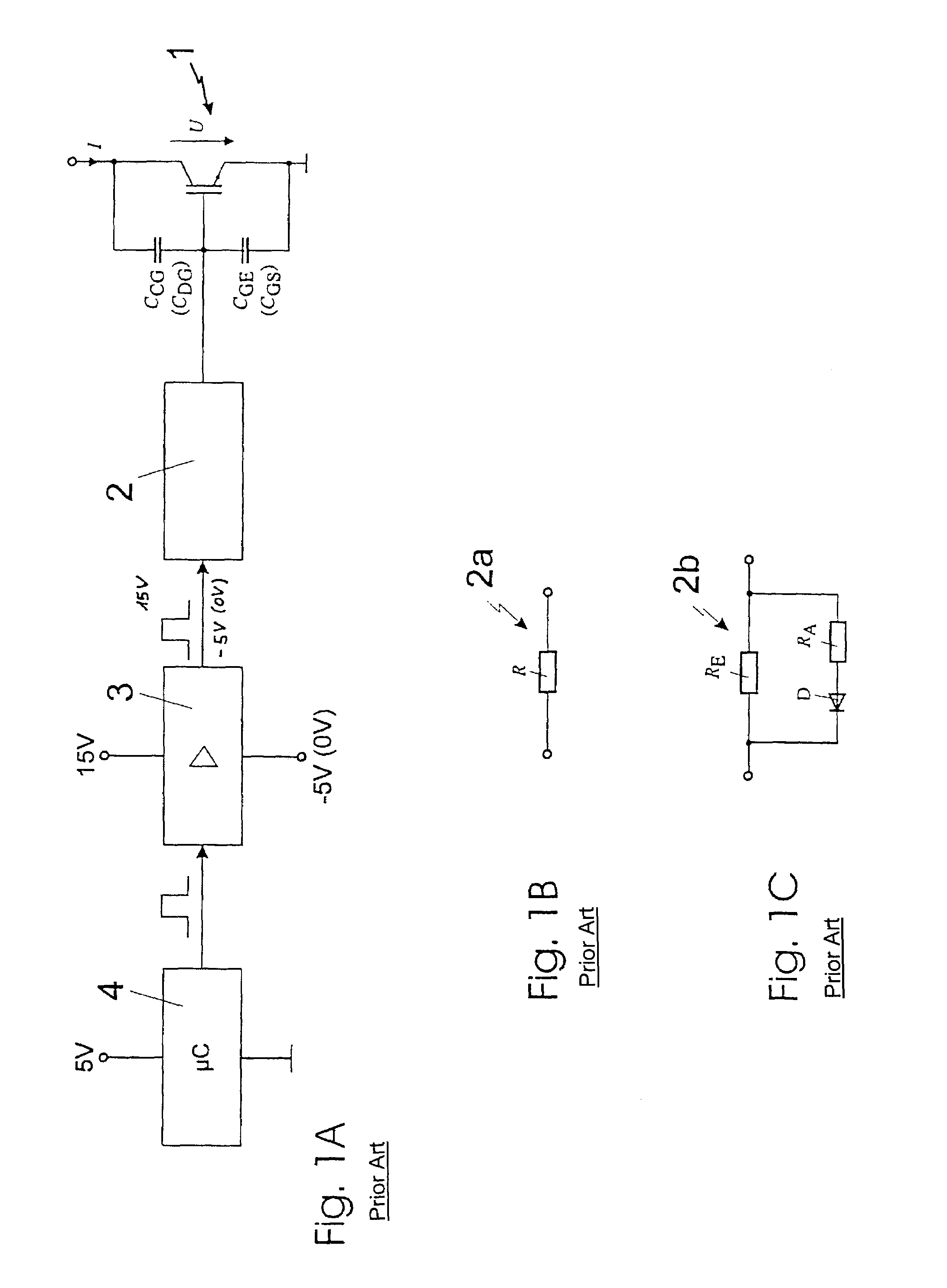
[0179]FIG. 1 on a highly schematic level shows a block diagram with a power semiconductor 1 which may be either an IGBT or a MOS-FET. A current I flows through power semiconductor 1 and a voltage U appears across the latter. For an IGBT, the input capacitance of the power semiconductor 1 corresponds to the gate-emitter capacitance CGE in parallel to the effective feed-back capacitance CCG. The effective feedback capacitance CCG is a function of the collector emitter voltage UCE.

[0180]For a MOS-FET the input capacitance of semiconductor 1 corresponds to the gate-source capacitance CGS.

[0181]Power semiconductor 1 is inputted via a network 2, two prior art embodiments of which being shown in FIGS. 1B and 1C.

[0182]Network 2 is controlled by an output stage 3 which, in turn, receives its signals from a micro-controller 4.

[0183]Micro-controller 4 conventionally has a supply voltage of 5 V and outputs control signals at TTL-level. Output stage 3 has a supply voltage of conventionally 0 / 15 ...


PUM


Abstract

A method and device for switching power semi-conductors on and off, especially for IGBTs and MOS-FETs with inductive loads, and how they would be employed with torque-variable asynchronous machines, in ignition systems for spark ignition engines, in switch mode power supplies and power factor controllers. During a switching operation of the power semiconductor, a voltage across the semiconductor and the current through the semiconductor are measured, a time function of the voltage as well as a time function of the current are controlled, and the control of the voltage time function and the control of the current time function are effected essentially one after the other.

Description

RELATED APPLICATIONS[0001]This application claims the right of priority under 35 U.S.C. §120, as authorized by 35 U.S.C. §365(c) to International Application No. PCT / EP01 / 14226 filed on Dec. 5, 2001 by the same inventors (published under PCT Article 21(2) in German and not English), which claims priority to Application No. 100 61 563.5 filed in Germany on Dec. 6, 2000, both of which are incorporated herein by reference in their entirety.FIELD OF THE INVENTION[0002]The present invention relates to the field of switching power semiconductors. More specifically, the invention is related to methods and apparatuses for switching power semiconductors, in particular power transistors, insulated gate bipolar transistors (IGBTs) and metal oxide field effect transistors (MOS-FETs).[0003]The present invention is preferably used for controlling electric induction motors at variable speeds, for operating ignition circuits in internal combustion engines, and for operating switched-mode power supp...

Claims


Application Information

Patent Timeline
IPC IPC(8): H03K3/00H03K17/16
CPCH03K17/168H03K17/166
Inventor MELBERT, JOACHIMDÖRLEMANN, CHRISTOPH
Owner RUBITEC GES FUR INNOVATION & TECH DER RUHR UNIV BOCHUM
Learn More