Method of making microelectronic spring contact array

a technology of spring contact array and spring contact, which is applied in the direction of individual semiconductor device testing, semiconductor/solid-state device testing/measurement, instruments, etc., can solve the problems of slowing down the process of making an array, limiting the use of tungsten wire and like components, and limited contact arrays with relatively few contacts

Inactive Publication Date: 2006-05-23
FORMFACTOR INC
View PDF23 Cites 73 Cited by
  • Summary
  • Abstract
  • Description
  • Claims
  • Application Information

AI Technical Summary

Problems solved by technology

Techniques using tungsten wire and like components are generally limited to contact arrays with relatively few contacts, because of practical difficulties associated with achieving and maintaining a precise contact tip alignment across the array.
The shape of composite contacts is somewhat limited by the wire shaping process.
This may slow down the process of making an array, particularly for a...

Method used


Image

  • Method of making microelectronic spring contact array
  • Method of making microelectronic spring contact array
  • Method of making microelectronic spring contact array

Examples


Embodiment Construction

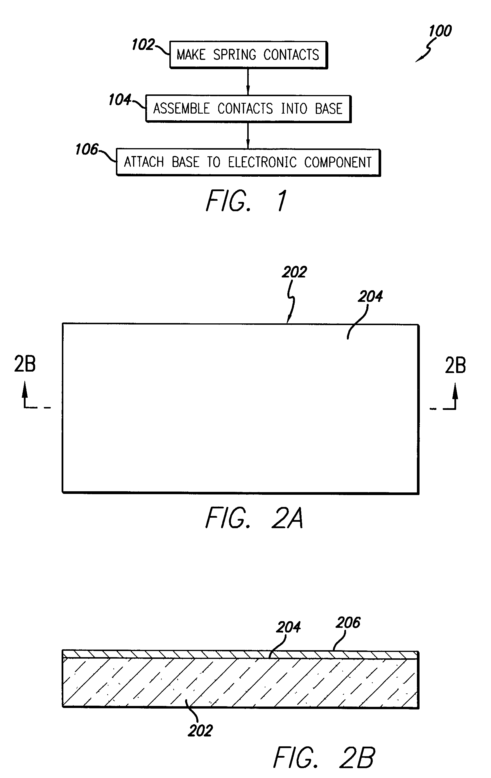
[0032]The present invention provides a method of making a microelectronic spring contact array that overcomes the limitations of prior art methods. In the detailed description that follows, like element numerals are used to indicate like elements appearing in one or more of the figures.

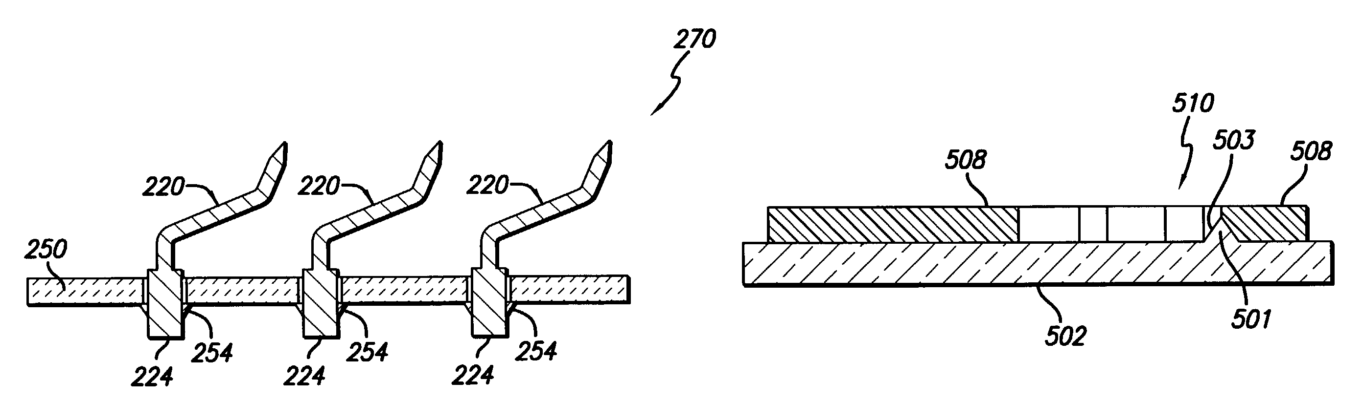
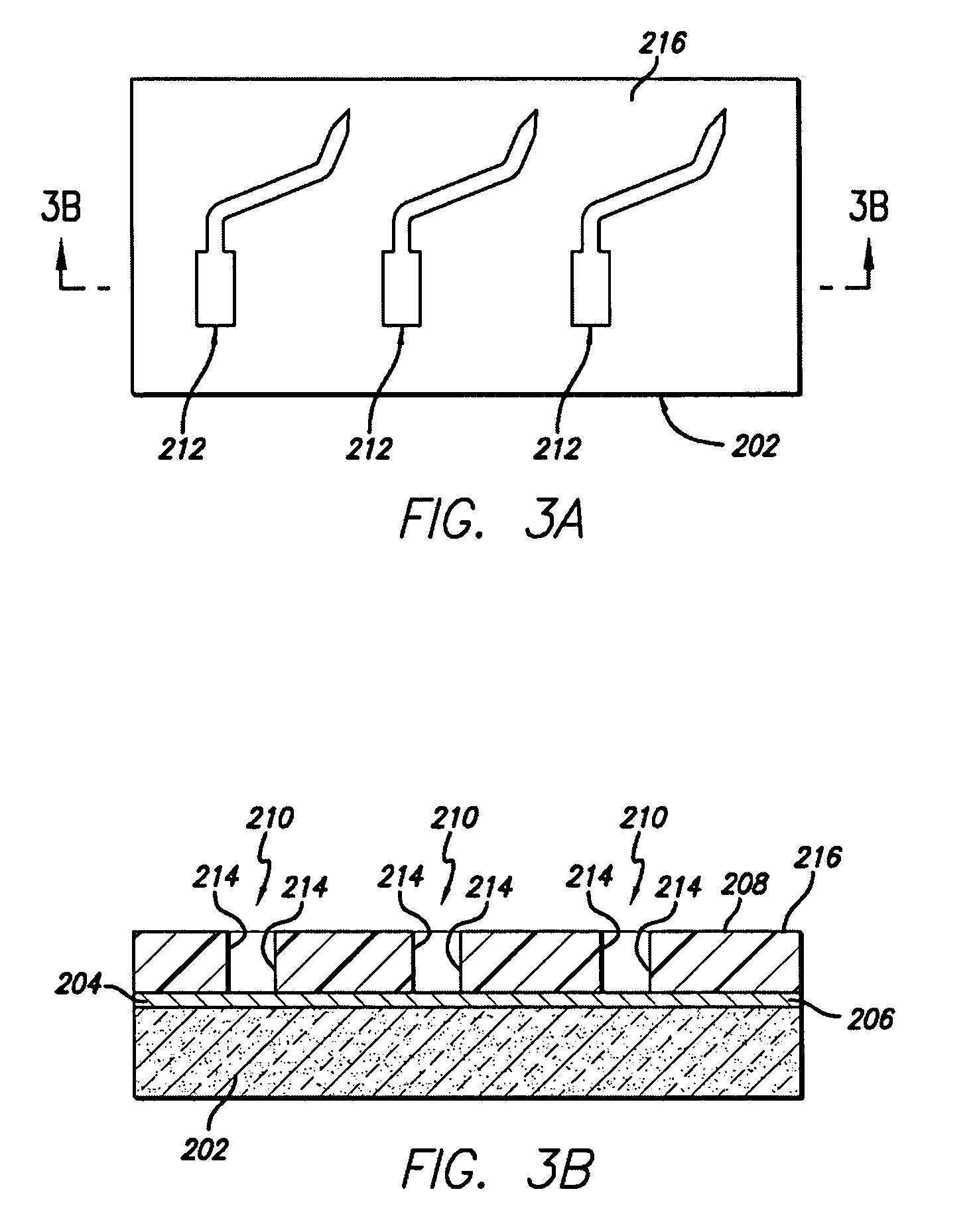
[0033]Spring contacts arrays made using a method according to the invention may be especially suitable for contacting very compact semiconductor devices, such as, for example, devices with terminals arranged at a pitch (average array spacing) of less than 5 mils (about 130 μm). The invention is also suitable for producing wiping-type spring contacts having elongated beams, for example, beams with an aspect ratio (ratio of length to width) of 3 or greater, and more typically, 10 or greater. The method may be used to produce straight or contoured beams having very precise dimensions and performance characteristics. While the method is especially suitable for making these types of spring contacts, it may...


PUM

PropertyMeasurementUnit
Thicknessaaaaaaaaaa
Electrical conductivityaaaaaaaaaa
Structureaaaaaaaaaa

Abstract

A method of making a microelectronic spring contact array comprises forming a plurality of spring contacts on a sacrificial substrate and then releasing the spring contacts from the sacrificial substrate. Each of the spring contacts has an elongated beam having a base end. The method of making the array includes attaching the spring contacts at their base ends to a base substrate after they have been released entirely from the sacrificial substrate, so that each contact extends from the base substrate to a distal end of its beams. The distal ends are aligned with a predetermined array of tip positions. In an embodiment of the invention, the spring contacts are formed by patterning contours of the spring contacts in a sacrificial layer on the sacrificial substrate. The walls of patterned recesses in the sacrificial layer define side profiles of the spring contacts, and a conductive material is deposited in the recesses to form the elongated beams of the spring contacts.

Description

BACKGROUND OF THE INVENTION[0001]1. Field of the Invention[0002]The present invention relates to methods of making microelectronic spring contact arrays, such as contact arrays for connecting to semiconductor devices (singulated or unsingulated), for purposes of testing or assembly.[0003]2. Description of Related Art[0004]Microelectronic spring contact arrays such as used for contacting C4 or flat pad terminals of semiconductor devices have previously been made in various different ways. Some older techniques involve the assembly of fine, stiff components, such as tungsten wires, onto a base, such as a probe card. Techniques using tungsten wire and like components are generally limited to contact arrays with relatively few contacts, because of practical difficulties associated with achieving and maintaining a precise contact tip alignment across the array.[0005]A more recent method, involving forming composite spring contacts on a substrate using a relatively soft, fine wire that is...

Claims


Application Information

Patent Timeline
IPC IPC(8): H01R43/00G01R31/26G01R1/067G01R1/073G01R3/00
CPCG01R1/06744G01R3/00G01R1/06733Y10T29/49222Y10T29/49224Y10T29/49139Y10T29/49208Y10T29/49204Y10T29/49155H01L22/00G01R1/067
Inventor ELDRIDGE, BENJAMIN N.MATHIEU, GAETAN L.REYNOLDS, CARL V.
Owner FORMFACTOR INC
Why Eureka
Try Eureka