

Device and method for cleaning articles used in the production of semiconductor components
- Summary
- Abstract
- Description
- Claims
- Application Information
AI Technical Summary
Benefits of technology
Problems solved by technology
Method used
Image

Examples
Embodiment Construction
[0016]This is where the exemplary embodiments intervene, being based on the object of providing measures with which the levels of scrap caused by impurities in the fabrication of semiconductor components can be reduced with the minimum possible outlay. One aspect of the exemplary embodiments is to take up the minimum possible footprint, and it is to be possible for the cleaning to be performed efficiently.
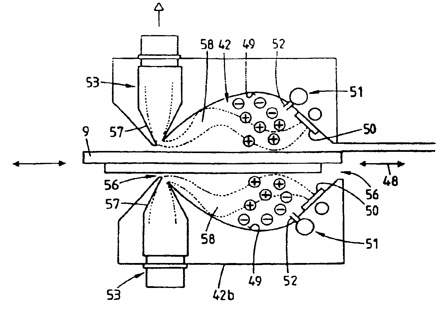
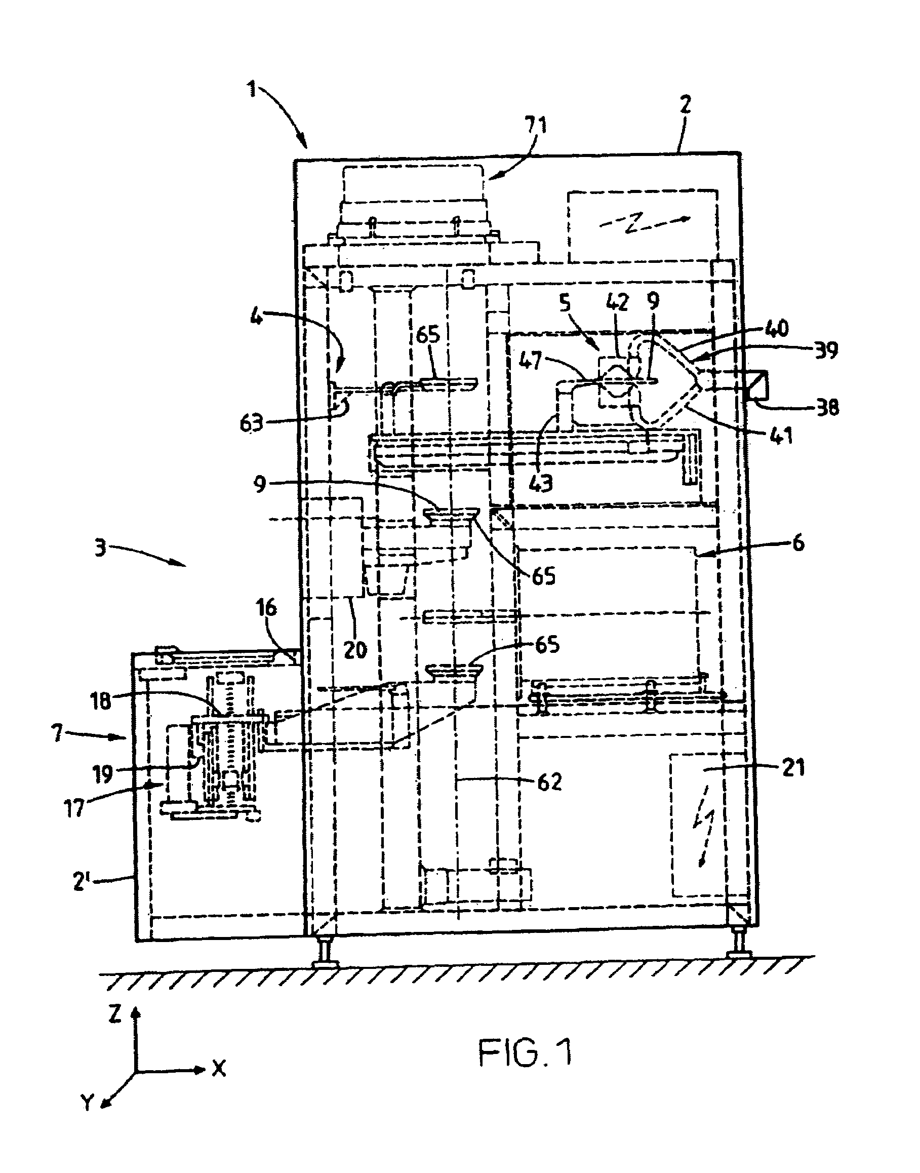
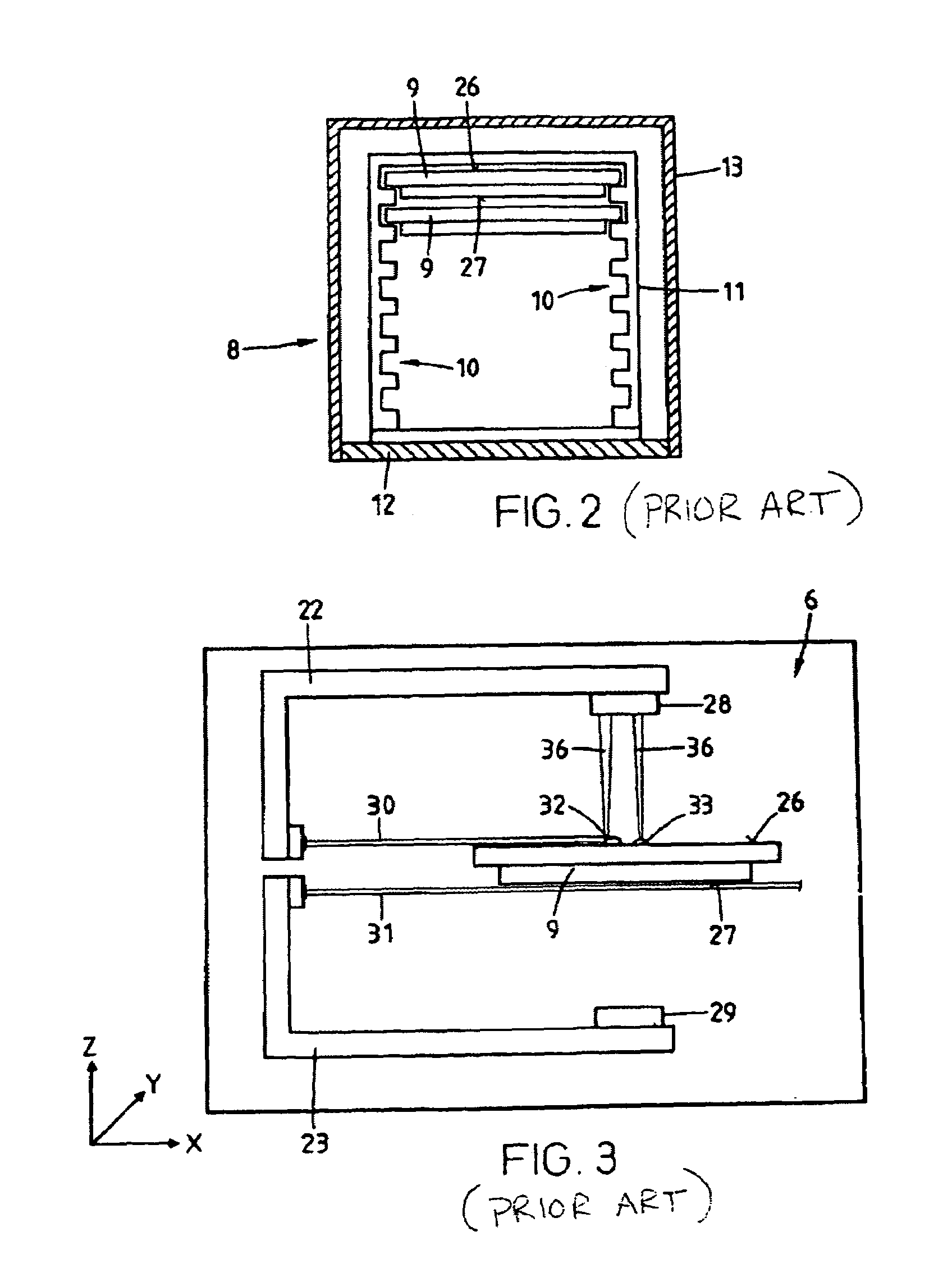
[0017]Therefore, the exemplary embodiments propose a cleaning apparatus for semiconductor component production, which is provided with two feed devices, each of which can be used to guide fluid medium over in each case once surface of an object which is to be cleaned, in particular of a semiconductor production means, so that different sides of the object can be cleaned simultaneously, at least two gas feed devices for introducing a cleaning gas which is under super atmospheric pressure opening out into a cleaning chamber, the gas feed devices each having a means for directing a ga...
PUM
| Property | Measurement | Unit |
|---|---|---|
| Thickness | aaaaa | aaaaa |
| Angle | aaaaa | aaaaa |
| Flow rate | aaaaa | aaaaa |
Abstract
Description
Claims
Application Information