Interconnect for microelectronic structures with enhanced spring characteristics

a microelectronic structure and spring technology, applied in the field of interconnection elements, can solve the problems of reducing the deflection required to permanently deform the interconnection element, and achieve the effect of increasing the spring constant of the interconnection element, increasing the resiliency, and measurable amount of resiliency

Inactive Publication Date: 2006-05-23
FORMFACTOR INC
View PDF32 Cites 102 Cited by
  • Summary
  • Abstract
  • Description
  • Claims
  • Application Information

AI Technical Summary

Benefits of technology

[0019]According to the invention, the spring constant of an interconnection element can be increased by coupling (e.g., coating) a second material over the first material. The first material is, for example, a body of the interconnection element formed to have some measurable amount of resiliency. The interconnection element of the invention increases this resiliency by coupling a second material that itself comprises resilient properties. The second material may also be used to increase the spring constant of a resilient interconnection. An increased spring constant permits the interconnection element of the invention to sustain a desired contact force to effect reliable pressure contact to an electronic component, making the interconnection element suitable for use in a variety of applications, including as part of a densely-packed array of interconnection elements on an electronic component to couple to a corresponding array of contact pads or terminals on a second electronic component. The addition of the second structure to the first structure will generally increase the working force for a given deflection, but may decrease the deflection required to permanently deform the interconnection element. The addition of the second structure may also increase or decrease the longevity of the interconnection element for a number of compression cycles to failure of the interconnection element, depending on the material properties of the structure material. In general, the ratios of the yield stress, σ, and elastic modulus, E, of the two structures along with the thickness of the structures (and the total thickness of the interconnection element) will determine the final outcome.

Problems solved by technology

The addition of the second structure to the first structure will generally increase the working force for a given deflection, but may decrease the deflection required to permanently deform the interconnection element.

Method used


Image

  • Interconnect for microelectronic structures with enhanced spring characteristics
  • Interconnect for microelectronic structures with enhanced spring characteristics
  • Interconnect for microelectronic structures with enhanced spring characteristics

Examples


Embodiment Construction

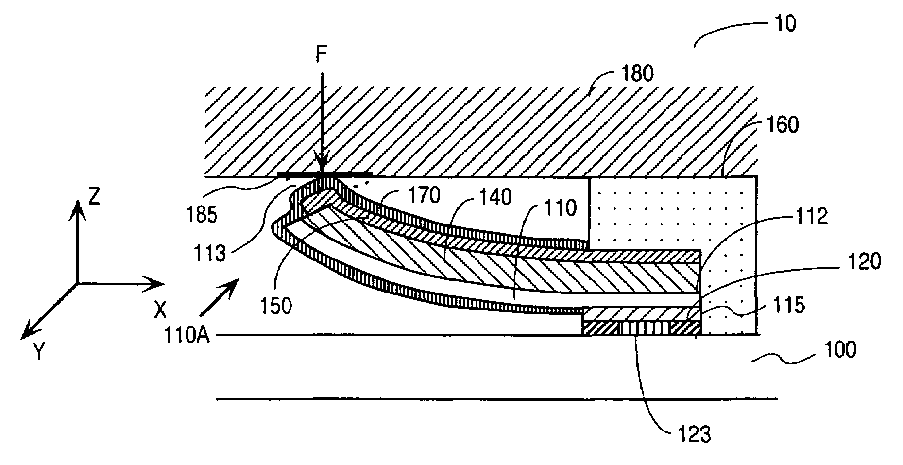
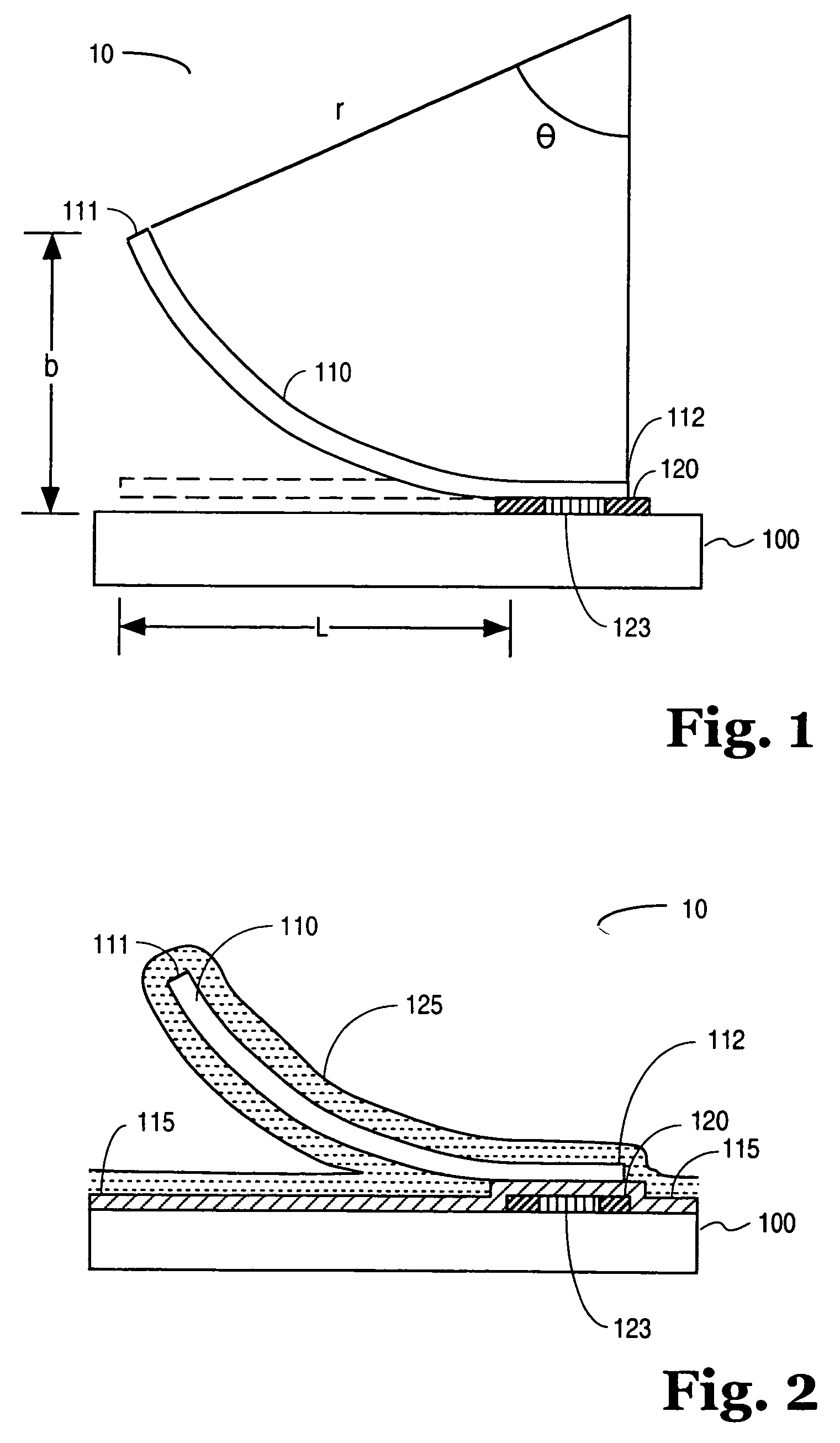
[0038]The invention relates to interconnection elements, including contact elements. According to one aspect of the invention, the invention contemplates an interconnection element with improved spring properties over prior art interconnection elements. In another aspect, the invention relates to improving the spring constant of prior art interconnection elements through the coupling of additional resilient material(s) to an existing interconnection element. In the either aspect, the invention describes an improved interconnection element over prior art interconnection elements thus improving the suitability of the interconnection element of the invention for use in present and future, reduced-sized applications, including providing a conductive path between electronic components such as in contacting and / or testing of contact pads or terminals of an electronic component.

[0039]Suitable electronic components include, but are not limited to, an active semiconductor device made of any ...


PUM

PropertyMeasurementUnit
heightaaaaaaaaaa
heightaaaaaaaaaa
thicknessaaaaaaaaaa

Abstract

An interconnection element and a method of forming an interconnection element. In one embodiment, the interconnection element includes a first structure and a second structure coupled to the first structure. The second structure coupled with the first material has a spring constant greater than the spring constant of the first structure alone. In one embodiment, the interconnection element is adapted to be coupled to an electronic component tracked as a conductive path from the electronic component. In one embodiment, the method includes forming a first (interconnection) structure coupled to a substrate to define a shape suitable as an interconnection in an integrated circuit environment and then coupling, such as by coating, a second (interconnection) structure to the first (interconnection) structure to form an interconnection element. Collectively, the first (interconnection) structure and the second (interconnection) structure have a spring constant greater than a spring constant of the first (interconnection) structure.

Description

[0001]This is a Divisional application of Ser. No. 09 / 473,414, filed Dec. 28, 1999 (now U.S. Pat. No. 6,827,584).BACKGROUND OF THE INVENTION[0002]1. Field of the Invention[0003]The invention relates to an interconnection element suitable for effective pressure connections between electronic components.[0004]2. Description of Related Art[0005]Interconnection or contact elements may be used to connect devices of an electronic component or one electronic component to another electronic component. For example, an interconnection element may be used to connect two circuits of an integrated circuit chip or to connect an application specific integrated circuit (ASIC) to another component such as a printed circuit board. Interconnection elements may also be used to connect the integrated circuit chip to a chip package suitable for mounting on a printed circuit board of a computer or other electronic device. Interconnection elements may further be used to connect the integrated circuit chip ...

Claims


Application Information

Patent Timeline
Patent Type & Authority Patents(United States)
IPC IPC(8): H01R12/00H01L21/48H01L23/48H01L23/485H01R13/24
CPCG01R1/06727G01R3/00H01L21/4853H01L24/11H01L24/13H01L24/16H01L24/72H01R12/57H01R13/03H05K3/4092Y10T29/49222H01L24/71H01L2224/11002H01L2224/11003H01L2224/13099H01L2924/01011H01L2924/01013H01L2924/01018H01L2924/01022H01L2924/01027H01L2924/01029H01L2924/01039H01L2924/0104H01L2924/01042H01L2924/01046H01L2924/01061H01L2924/01074H01L2924/01078H01L2924/01079H01L2924/01082H01L2924/10329H01L2924/14H01L2924/1433H01L2924/3011H01R13/24H05K3/326H05K2201/0311H01R12/718H01L2924/01005H01L2924/01006H01L2924/01019H01L2924/01033H01L2924/01045H01L2924/01072H01L2924/014H01L2924/0001G01R1/06761Y10T29/49204Y10T29/49147Y10T29/49149Y10T29/49224G01R1/06711H01L2224/05001H01L2224/05568H01L2224/11H01L2224/13H01L2224/13155H01L2224/13171H01L2224/136H01L2224/16H01L2924/12042H01L2924/15787Y10T29/49126Y10T29/49155H01L2924/00H01L2924/00014H01L2924/00012
Inventor MATHIEU, GAETAN L.ELDRIDGE, BENJAMIN N.
Owner FORMFACTOR INC
Why Eureka
Try Eureka