Active inductance circuit and differential amplifier circuit

a technology of active inductance and differential amplifier, which is applied in the direction of network simulating reactance, multiple-port active network, frequency selective two-port network, etc., can solve the problems of reduced logic that can be carried on the chip, increased cost due to chip size increase, and reduced inductance located in the chip fabricated by using wiring layers. , to achieve the effect of reducing the number of elements and small voltage drop

Inactive Publication Date: 2006-05-23
RENESAS ELECTRONICS CORP
View PDF4 Cites 12 Cited by
  • Summary
  • Abstract
  • Description
  • Claims
  • Application Information

AI Technical Summary

Benefits of technology

[0010]With the foregoing in view, it is an object of the present invention to provide an active inductance circuit with reduced number of elements. It is another object of the present invention to provide an active inductance circuit i

Problems solved by technology

However, an inductance located in a chip fabricated by using wiring layers requires a large surface area even in the case of a small inductance value.
As a result, cost is raised due to increase in the chip size, and logic that can be carried

Method used


Image

  • Active inductance circuit and differential amplifier circuit
  • Active inductance circuit and differential amplifier circuit
  • Active inductance circuit and differential amplifier circuit

Examples


first embodiment

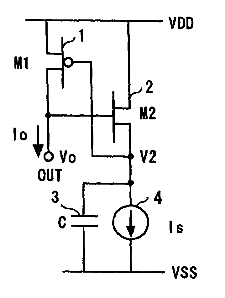
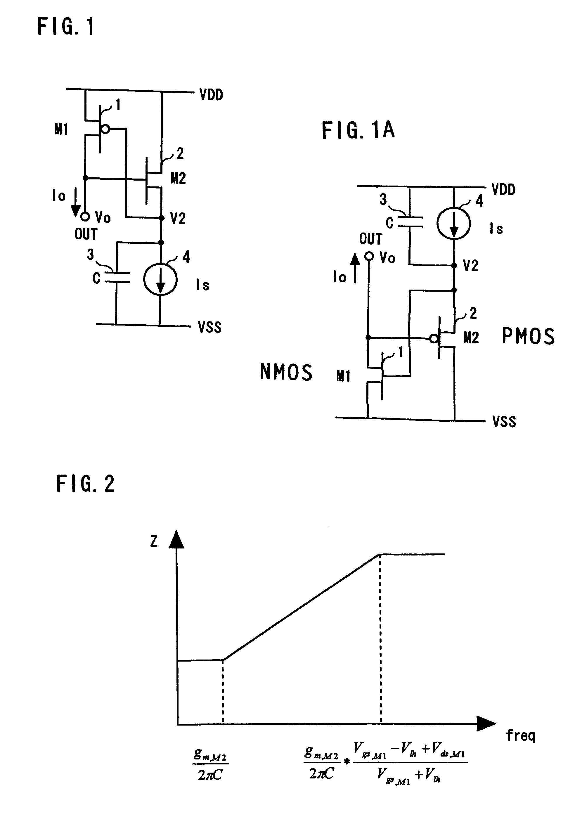
[0033]FIG. 1 shows the first embodiment of the active inductance circuit in accordance with the present invention. In FIG. 1, the source of a P-type MOS transistor M1(1) is connected to a high-voltage power source VDD and the drain is connected to an output terminal OUT. The drain of an N-type MOS transistor M2(2) is connected to the VDD directly or via an element for protection against surge. The source of the N-type MOS transistor M2(2) is connected to a current source 4. The gate of the N-type MOS transistor M2(2) is connected to the drain of the P-type MOS transistor M1(1) or to the output terminal OUT, thereby forming a source follower circuit.

[0034]The current source 4 is connected to a low-voltage power source VSS. The gate of the MOS transistor M1(1) and a capacitor 3 are connected to the source of the NMOS transistor M2(2). The other terminal of the capacitor 3 is connected to the VSS. The capacitor 3 and current source 4 are connected in parallel between the source of the ...

second embodiment

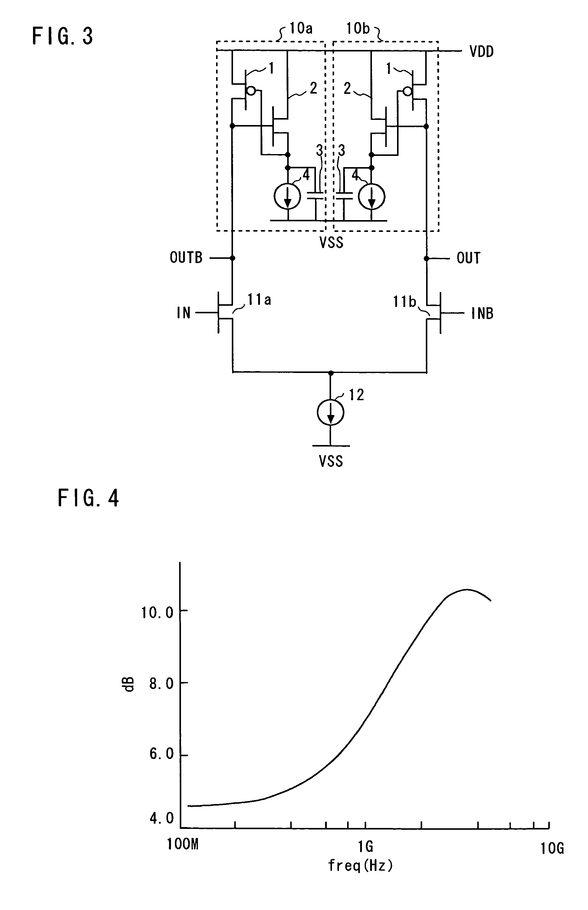
[0050]FIG. 3 is a circuit diagram illustrating the configuration of the differential amplifier circuit of the second embodiment. Referring to FIG. 3, NMOS transistors 11a and 11b constitute a differential pair and are commonly connected at the source side and connected to a current source 12. The current source 12 is connected to a low-voltage power source VSS. Gates of the NMOS transistors 11a and 11b are connected to input terminals IN and INB. The active inductors 10a and 10b that have been explained with reference to FIG. 1 are connected to drains of NMOS transistors 11a and 11b, respectively. Drains of PMOS transistors M2(2) of respective active inductors 10a and 10b are connected to respective drains of NMOS transistors 11a and 11b.

[0051]In other words, the drains of NMOS transistors 11a and 11b are connected to respective output terminals of the active inductors 10a and 10b, the nodes are connected to output terminals OUTB and OUT, and signals are outputted. The IN and OUTB ...

third embodiment

[0054]FIG. 5 is a circuit diagram illustrating the configuration of the differential high-pass amplifier circuit of the third embodiment. Referring to FIG. 5, NMOS transistors 11a and 11b constitute a differential pair, and current sources 12a and 12b are connected to respective sources of NMOS transistors 11a and 11b. The current sources 12a and 12b are connected to a low-voltage power source VSS. Further, a capacitor 13 is connected between the sources of NMOS transistors 11a and 11b. The active inductors 10a and 10b that have been explained with reference to FIG. 1 are connected to drains of NMOS transistors 11a and 11b, respectively.

[0055]The connection mode of active inductors 10a and 10b and NMOS transistors 11a and 11b is identical to that of the second embodiment. Using such a circuit configuration makes it possible to realize a high-pass amplifier in which a gain in a low-frequency region is further suppressed. A resistor can be used as impedance instead of the capacitor 13...


PUM


Abstract

An active inductance circuit comprising a signal terminal (OUT) and having voltage and current characteristics, as viewed from this terminal, which are identical to those of a circuit comprising an inductance, this active inductance circuit having a structure in which the drain terminal of a first MOS transistor M1 and the gate terminal of a second MOS transistor M2 different in conductivity type from the first MOS transistor are connected to the signal terminal, the gate terminal of the first MOS transistor is connected to the source terminal of the second MOS transistor, a capacitor and a current source are connected to the source terminal of the second transistor, the source terminal of the first MOS transistor and the drain terminal of the second MOS transistor are connected to a power source and other terminals of the capacitor and current source are connected to another power source.

Description

BACKGROUND OF THE INVENTION[0001]1. Field of the Invention[0002]The present invention relates to an active inductance circuit having transistors and a capacitor and operating as an inductance and to a differential amplifier circuit having the circuit.[0003]2. Description of the Related Art[0004]Inductances have been widely used with the object of extending an amplification band and compensating transmission characteristics in high-speed communication circuits. However, an inductance located in a chip fabricated by using wiring layers requires a large surface area even in the case of a small inductance value. As a result, cost is raised due to increase in the chip size, and logic that can be carried on the chip is decreased. To overcome this problem, active inductance circuits in which active elements such as transistors and passive elements such as capacitors are combined to have characteristics equivalent to an inductance have been suggested[0005]An example of such an active induct...

Claims


Application Information

Patent Timeline
IPC IPC(8): H03F3/45H03H11/00H03H11/04H03H11/48
CPCH03F3/45381H03F3/45394H03F1/483H03H11/48H03F2203/45488H03F2203/45631H03F2203/45641H03F2203/45648H03F2203/45632
Inventor SODA, MASAAKI
Owner RENESAS ELECTRONICS CORP
Why Eureka
Try Eureka