Amplifier bias enhancement technique

a technology of amplifier bias and amplifier, applied in the direction of amplifier, gain control, high-frequency amplifier, etc., can solve the problems of long battery life, inconvenient optimum linearity and low noise operation, and input port of the lna

Active Publication Date: 2006-05-23
SIGE SEMICON
View PDF7 Cites 8 Cited by
  • Summary
  • Abstract
  • Description
  • Claims
  • Application Information

AI Technical Summary

Benefits of technology

[0006]In accordance with the invention there is provided a method of increasing an auto bias effect for an amplifier circuit comprising: receiving of a RF input signal; providing an amplifier circuit having at least a first transistor; providing a bias boost circuit for providing a variable bias current; amplifying of the RF input signal using the amplifier circuit and the at least a first transistor to form a RF output signal; receiving a portion of the RF output signal; and, biasing of the at least a first transistor of the amplifier circuit using the variable bias current in dependence upon the received portion of the RF output signal power.
[0007]In accordance with the invention there is provided a method of increasing an auto bias effect for an amplifier circuit comprising: receiving of a RF input signal; providing an amplifier circuit having at least a first transistor and a biasing circuit for biasing of the first transistor; providing a bias boost circuit for providing a variable bias current; amplifying of the RF input signal using the amplifier circuit and the at least a first transistor to form a RF output signal; using a portion of the RF output signal to autobias the biasing circuit for biasing of the amplifying transistor; and, biasing of the at least a first transistor of the amplifier circuit using the bias boost circuit that is autobiased by the portion of the signal power of the RF output signal.

Problems solved by technology

Unfortunately, in battery-operated equipment, this large bias current is not conducive to long battery life, it is also not conducive to optimum linearity and to low noise operation.
However, where the active LNA device is in close proximity to the transmitter, for example as in an antenna-coupled LNA, situations may arise where the input signal provided to the input port of the LNA causes overload because it has a high signal power.
LNAs typically have low gain, but, often do not have the low noise performance when biased for best linearity.
Conversely, they often do not have best linearity when biased for lowest noise.
PAs on the other hand, typically have low gain when deliberately biased at low currents.
This effect, however, is limited and there exists a need to provide a means to enhance the autobias effect and improve linearity with even stronger input signals.

Method used


Image

  • Amplifier bias enhancement technique
  • Amplifier bias enhancement technique
  • Amplifier bias enhancement technique

Examples


Embodiment Construction

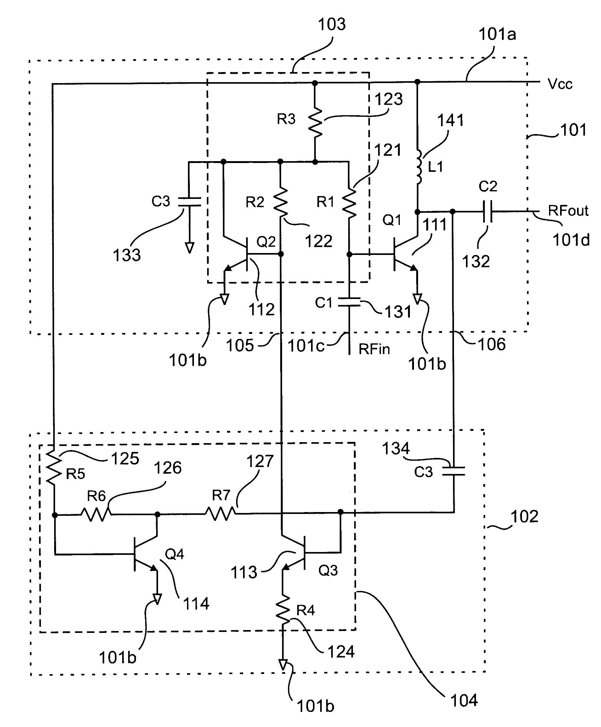
[0012]FIG. 1 illustrates a state of the art amplifier circuit 101 as well as a bias boost circuit 102, in accordance with an embodiment of the invention. A first transistor Q1111 is the predominant amplification transistor and is used for amplifying of a RF input signal that is received from an input port 101c to form an amplifier version of the input signal as a RF output signal at an output port 101d. A coupling capacitor C1131 is used to couple of this RF input signal to the base terminal of transistor Q1111. Optionally, a more advanced coupling network is disposed between the base terminal of transistor Q1111 and the input port 101c for coupling of the RF input signal.

[0013]Choke L1141 is disposed between the collector terminal of transistor Q1111 and the first supply voltage port 101a. This choke L1141 provides a high impedance path to the collector terminal of transistor Q1111. Capacitor C2132 is disposed between the collector terminal of transistor Q1111 and the output port 1...


PUM


Abstract

A bias boost circuit is disclosed for use with an amplifier circuit for biasing thereof. The amplifier circuit includes at least a first transistor and a filter circuit for filtering of current pulses received from the bias boost circuit, where filtered current pulses form a variable bias current that is provided to the at least a first transistor. With this type of biasing circuit, large input signals that would normally compress the gain of the amplifier circuit are therefore amplified with less gain compression by virtue of the boost in bias current that is supplied to the at least a first transistor.

Description

FIELD OF THE INVENTION[0001]The invention relates to the field of amplifier circuits and more specifically to the field of bias boost circuits for use with amplifier circuits.BACKGROUND OF THE INVENTION[0002]RF power amplifiers (PAs) are typically used for propagating amplitude and phase information for a RF input signal in an accurate manner so as not to corrupt data being transmitted within the RF signal. Generally, in order to attain this accuracy, a large bias current is used to bias the PA at an operating point with sufficient gain and bandwidth. Unfortunately, in battery-operated equipment, this large bias current is not conducive to long battery life, it is also not conducive to optimum linearity and to low noise operation.[0003]Low noise amplifiers (LNA) are typically biased at a fixed current for minimum noise operation so that small amplitude input signals are detectable. In determining the bias point for an active device performing signal amplification, there is a trade-o...

Claims


Application Information

Patent Timeline
Patent Type & Authority Patents(United States)
IPC IPC(8): H03G3/10H03F1/26H03F1/30H03F1/32H03F3/189H03F3/343
CPCH03F1/302H03F3/3432H03F2200/372H03F2200/294
Inventor YUEN, GREGORY
Owner SIGE SEMICON
Why Eureka
Try Eureka