Flip-chip package and fabricating process thereof

a technology of flip-chip and fabrication process, which is applied in the direction of sustainable manufacturing/processing, final product manufacturing, printed circuit aspects, etc., can solve the problems of relative complexity and cost in fabrication, the equipment for fabricating solder bumps is quite expensive, and the fabricating process is relatively complicated, so as to reduce the number of steps and the cost of fabrication.

Active Publication Date: 2006-05-30
ADVANCED SEMICON ENG INC
View PDF5 Cites 78 Cited by
  • Summary
  • Abstract
  • Description
  • Claims
  • Application Information

AI Technical Summary

Benefits of technology

[0008]In view of the forgoing, this invention provides a flip-chip package and a process for fabr

Problems solved by technology

Ordinary types of bump include solder bump, gold bump, electrically conductive adhesive bump and polymer bump, wherein the solder bump is the most popular one, but is also relatively complicated and expensive in f

Method used


Image

  • Flip-chip package and fabricating process thereof
  • Flip-chip package and fabricating process thereof
  • Flip-chip package and fabricating process thereof

Examples


Embodiment Construction

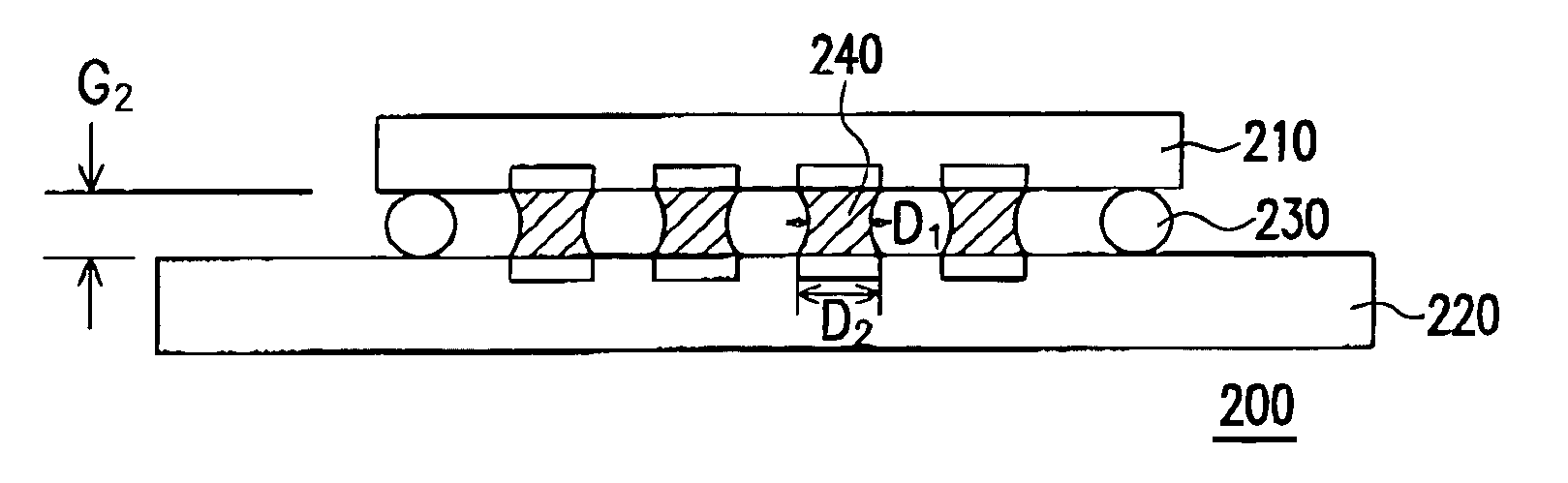
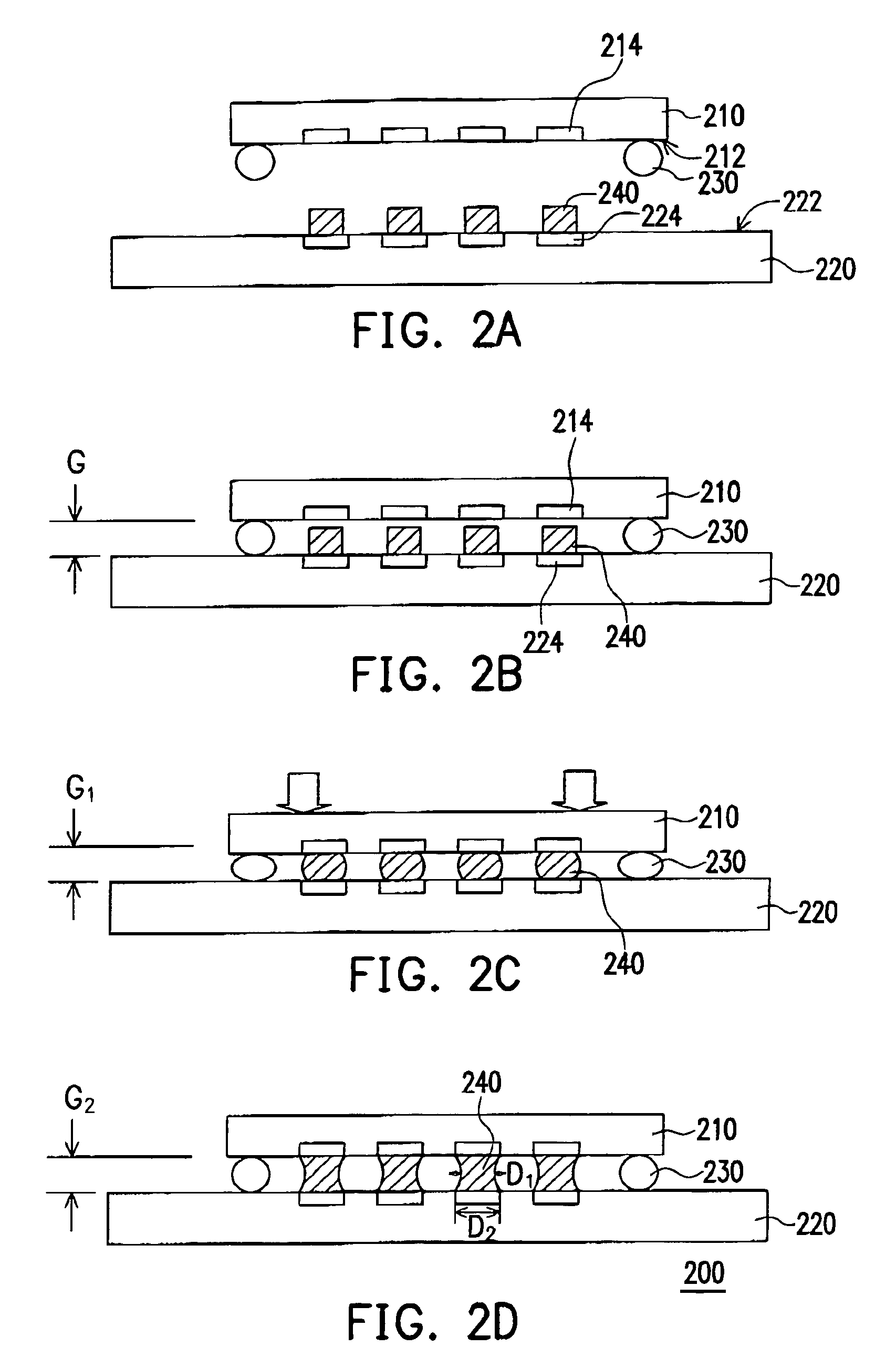
[0017]FIGS. 2A–2D illustrate a process flow of fabricating a flip-chip package according to the preferred embodiment of this invention. Referring to FIG. 2A, a chip 210 having an active surface 212 with bonding pads 214 disposed thereon is provided, and supporters 230 are disposed at the periphery of the active surface 212 of the chip 210. The supporters 230 may be disposed outside the four corners of the active surface 212, and are formed as gold bumps, for example. Each gold bump can be formed by, for example, bonding a gold wire to the chip 210 with a wire bonding method, and then pulling the gold wire apart to leave a portion thereof on the chip 210 as a gold bump. During the wire-bonding step, a portion of each softened gold wire can be extruded into a spherical gold bump by using an existing fully-developed wire bonding apparatus, and then the other portion of the gold wire is pulled apart from the gold bump. Since the gold bumps are formed with an existing fully-developed wir...


PUM


Abstract

A flip-chip package is described. The flip-chip package includes a chip, a substrate, supporters and electrically conductive adhesive bumps. The electrically conductive adhesive bumps are located between the chip and the substrate electrically connecting the bonding pads on the former and the bump pads on the latter, wherein each electrically conductive adhesive bump has a smaller diameter at the central portion thereof than at the end portions thereof. The supporters are also disposed between the chip and the substrate surrounding the active area of the chip, so that the chip can be supported on the substrate.

Description

CROSS-REFERENCE TO RELATED APPLICATION[0001]This application claims the priority benefit of Taiwan application serial no. 92104000, filed on Feb. 26, 2003.BACKGROUND OF THE INVENTION[0002]1. Field of the Invention[0003]The present invention relates to a flip-chip package and a process for fabricating the same. More particularly, the present invention relates to a flip-chip package with electrically conductive adhesive bumps disposed between a chip and a substrate, and to a process for fabricating the same.[0004]2. Description of the Related Art[0005]Flip-chip (FC) interconnect technology has been widely used in the package industry because it facilitates reduction of package area, shortening of signal transmission paths, and fabrication of package structures having high pin counts. In a FC packaging process, a chip is provided with bonding pads disposed on the active surface thereof and arranged in an area array, and bumps are disposed on the bonding pads. Then, the chip is flipped ...

Claims


Application Information

Patent Timeline
IPC IPC(8): H01L21/44H01L21/56H01L21/60H01L23/485H05K3/30H05K3/32
CPCH01L24/81H01L24/83H05K3/303H01L24/17H01L24/29H01L24/13H01L21/563H01L2224/81136H01L2224/1134H01L2224/13099H01L2224/13144H01L2224/1319H01L2224/16225H01L2224/81801H01L2224/8319H01L2224/838H01L2924/01029H01L2924/01047H01L2924/01051H01L2924/01074H01L2924/01078H01L2924/01079H01L2924/0781H05K3/321H05K2201/0367H05K2201/2036H01L2924/00011H01L2224/81192H01L2224/10135H01L2224/81139H01L2924/00013H01L2224/29101H01L2924/0665H01L2924/014H01L2924/01033H01L2224/29298H01L2224/2919H01L2924/00H01L2224/29099H01L2224/29199H01L2224/29299H01L2224/2929H01L2224/45144H01L2224/05571H01L2224/05573H01L2224/05184Y02P70/50H01L2224/05647H01L2924/00014H01L2224/05144H01L2224/05155
Inventor PAI, TSUNG-MINGHSIEH, SHIN-SHYAN
Owner ADVANCED SEMICON ENG INC
Why Eureka
Try Eureka